This thread has been locked.

If you have a related question, please click the "Ask a related question" button in the top right corner. The newly created question will be automatically linked to this question.

ADS1291: ADS1291 Saturation Issue with -300mV DC Offset During Input Impedance Test on Modified ADS1x9xECG-FE Board

Part Number: ADS1291
Other Parts Discussed in Thread: ADS1292R, ADS1298, ADS1293

Tool/software:

Hello TI Team,

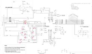
I’m currently evaluating the ADS1291 using the ADS1x9xECG-FE development board, which originally comes with the ADS1292R. For my use case, I’ve replaced the ADS1292R with the ADS1291 and made corresponding hardware modifications to work with channel 1 only. I’ve attached the updated schematic for reference.

The board is powered with a unipolar 3.0V AVDD, and I’m using the internal reference. The issue arises when I perform the input impedance test using Whaleteq’s SECG simulator, which applies:

  • LA: 1 mV, 1 Hz sine wave superimposed on a -300 mV DC offset

  • RA: 0 mV

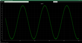
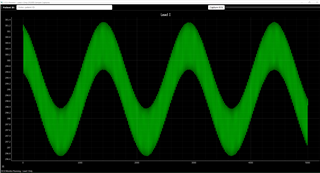
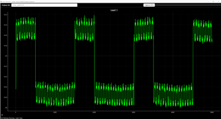
In this configuration, the ADS1291 saturates, and instead of a sine wave, I see a square waveform. Interestingly:

  • The sine wave is captured correctly if the DC offset is 0 mV or +300 mV.

  • To investigate further, I set the PGA gain to 1 and slowly varied the DC offset.

    • The signal works up to -20 mV DC offset.

    • Beyond -20 mV (even at -24 mV), the output saturates, and I get square pulses.

Further observations:

  • If I set PDB_REFBUF = 0 (turning off the internal reference buffer), the saturation issue disappears, but then I observe a constant offset around 2000 mV, likely due to the lack of a stable VREF.

  • Applying ±300 mV DC offset works fine when the reference buffer is disabled.

To isolate the issue, I tested the same SECG setup on:

  • A custom-built board using ADS1298 (also with 3.0V AVDD, internal reference)

  • An ADS1293-based board

Both these setups work perfectly under the same test conditions, with no saturation or clipping.

I’m including the register configuration I’m using for the ADS1291 below for your reference.

Register Configurations:

    writeRegister(0x1, 0x03);
    writeRegister(0x2, 0xA0);
    writeRegister(0x3, 0x10);
    writeRegister(0x4, 0x10);
    writeRegister(0x5, 0x90);
    writeRegister(0x6, 0x23);
    writeRegister(0x7, 0x00);
    writeRegister(0x8, 0x00);
    writeRegister(0xA, 0x03);

Could you help me understand why the ADS1291 behaves differently under these conditions compared to ADS1298 and ADS1293, despite the similar setup?

Thanks in advance for your support!

Best regards,
Sajin M.

  • Hello Sajin,

    Thank you for your post.

    What is establishing the input common-mode voltage for these tests? Given that you are using a unipolar 3V analog supply, the input common-mode is expected to be close to mid-supply or 1.5V. I believe you should be using the RLD amplifier to drive a mid-supply common-mode to your patient simulator. Without this, you will not be able to accurately measure signals with -300mV offset since this is below the AVSS supply (see Input Common-Mode Range in the ADS1291/2 data sheet).

    Using a mid-supply common-mode will shift the outputs of both RA and LA to the same DC level. After that is done correctly, you can enable the ±3mV sine wave input with ±300mV offset added to the LA output, which will give the necessary differential offset for the test.

    Regards,

    Ryan

  • Hi Ryan,

    Thank you for the reply. Yes I am using the RLD and with respect to ground it is around 1V. When you mention the common mode voltage of RA and LA means the voltage between RA-ground or RA-RLD? Can you please verify my register configuration is correct?

  • Hi Sajin,

    The common-mode is with respect to GND. Each electrode should have a mid-supply common-mode when RLD is regulating correctly.

    The register settings look ok. You can set 06h to 0x00 to remove the channel 1 inputs from the RLD common-mode sensing (unless it is required to test with the same configuration as the end product).

    Regards,

    Ryan