This thread has been locked.

If you have a related question, please click the "Ask a related question" button in the top right corner. The newly created question will be automatically linked to this question.

ADS114S08B: Single-Ended Inputs, PGA and VREF

Part Number: ADS114S08B
Other Parts Discussed in Thread: ADS114S08, ADS124S08

Tool/software:

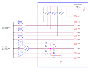
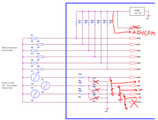
I am planning to use ADS114S08B to acquire 6 passive (resistance) and 3 active (voltage) single-ended inputs, all these inputs must be referred to GND (0V).

For passive inputs PGA is needed and the resistance source has to be feeded (pull-up) with the same VREF used by the converter (ratiometric acquisition). I think using the two internal IDACs is not applicable in this case (6 indipendent inputs).

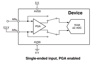
In this case I see that AVDD = +2.5V and AVSS = -2,5V in order to use the internal PGA, right?

AINCOM pin is to be connected to GND (0V) for single-ended inputs, right?

I cannot feed passive inputs with the internal 2.5V VREF: REFCOM pin should be connected to AVSS, so REFOUT voltage is near 0V referred to GND, right?

So I have to use an external reference 2.5V VREF to feed feed passive inputs and to be connected at REFP0 / REFN0 pins. Connecting REFP0 = +2.5V and REFN0 = GND (0V) is correct?

  • Hi Vagni,

    Can you put another "dummy" resistor in series with the resistance you are measuring - between the bottom of the sensor and ground - allowing you to take a differential measurement across the top resistor? Then you will be able to use the PGA and will not need bipolar supplies.

    It would help to see a drawing or block diagram of what you are trying to do so we can comment further on how you need to modify your circuit, or the ADC settings to use, to make it work

    -Bryan

  • Hi Bryan,

    Here is a block diagram of my analog single-ended inputs with their connections to the ADC I am thinking about.

    Each analog source must be independent from the others; they only have the common 0V reference.

    By resistance source I can measure thermistor resistance through a pullup and PGA for different value ranges, but also detect open-contact or closed-contact to GND. The DC positive voltage source is acquired through a voltage divider: for those inputs PGA = 1.

    How could be the best way (I hope it exists) to handles those inputs with ADS114S08B ?

  • Hi

    Why not do something like this instead?

    You can measure each thermistor differentially between REFOUT and the respective analog input (AIN0 to AIN5). I connected REFOUT to AINCOM in this case, so you set MUXP = AINCOM and MUXN = AIN0 to measure R1 for example

    Then you can add a third resistor in your resistor divider as shown and measure these inputs differentially as well. For example, you would set MUXP = AIN6 and MUXN = AIN9 to measure V1. You'd have to choose the resistor values, based on the expected voltages from your DC sources, so that the inputs are within the common-mode range of the ADC when the PGA is enabled (even when G=1)

    This should allow you to use the PGA in all cases because you are no longer measuring single-ended inputs. Or, at least the PGA can be enabled and gain = 1 so it basically acts as a buffer with some small headroom requirements. Then you don't need bipolar supplies either

    You also don't need to feed that internal reference voltage back into the ADC external reference pins, it's already internal!

    -Bryan

  • Hi Bryan,

    I understand you are referring to the following single-ended inputs scheme with PGA enabled, right?

    Then I can enable the internal 2.5V VREF, REFCOM = AVSS and REFOUT to feed AINCOM and all the resistance pullups.

    For measuring V1 differentially I can set the resistor divider in order to get VIN = VAINP - VAINN spanning from 0V (V1 = 0V) to VREF (V1 = Vmaxwith PGA = 1. I agree with you.

    But I do not understand how to measure for example R1 referred to AINCOM.Tipically R1 is generally variable in a limited range, so I need PGA > 1 quite always. FSR = VREF/PGA, so the RP pullup value should be related to the variable range of R1.

    But my resistance inputs must be configurabled for various resistance ranges and I cannot change RP each time, RP must be unique in my application.

    In this case VREF is enabled and used: using one of the the two internal IDACs switched to one resistance analog input at time may be more useful?

    Also, I look at VAINx common mode limits when PGA is enabled. For example, with PGA = 8 I get FSR = VREF/8. With AVSS = 0V and AVDD = +5V, VAINx,min = 150mV + VREF*(7/16) and VAINx,max = 4.85V - VREF*(7/16). And with PGA = 32 I get FSR = VREF/32, VAINx,min = 150mV + 15.5*VREF/32 and VAINx,max = 4.85V - 15.5*VERF/32. Is it correct?

  • Hi Vagni,

    Below is how I am interpreting the information you provided: you have a thermistor (NTC in this example) in series with a fixed resistance, and you are biasing this resistor divider circuit with the ADC REFOUT of 2.5V. I assumed the NTC has a nominal resistance of 10kohm, and the fixed resistor is also 10kohm. This gives you a voltage of REFOUT/2 whenever the temperature is at 25C. Of course you can pick whatever you like for your system

    • At the nominal temperature, the output voltage measured by the ADC is approximately 1.25V. You could use a maximum gain of 2 under these conditions, but to account for tolerances, gain error, etc., it's probably best to use gain = 1 in this case
    • When the temperature is less than nominal, the NTC resistance increases such that the output voltage measure by the ADC is <<1.25V. You could use a higher gain in this case, but somehow you'd have to detect this situation and dynamically change the gain. Typically most NTC measurement circuits I have seen just use a fixed gain as a result (usually a gain of 1)
    • When the temperature is greater than nominal, the NTC resistance decreases such that the output voltage measure by the ADC is now >1.25V. In this case you must use a gain of 1

    In all cases the absolute voltage on the ADC pins is within the recommended operating conditions, assuming the gain =1 and that the NTC resistance does not get arbitrarily low such that IN- is within 150mV of AVSS

    Here is what I was envisioning for the voltage measurements. I just quickly picked resistance values that would work based on the example input voltage (10V), you should calculate your own values based on your actual system requirements. But in the example below, you can use a gain of 1 with the PGA enabled and not have any issues

    You can reference the "CMR tool" in our ADS124S08 online calculator for help identifying if your input signals are within range. Note that the ADS124S08 is just the 24-bit version of the ADS114S08, and is otherwise functionally the same: 

    https://dev.ti.com/gallery/view/PADC/PADC_Design_Calculator_Tool/ver/1.20.0/

    -Bryan