This thread has been locked.

If you have a related question, please click the "Ask a related question" button in the top right corner. The newly created question will be automatically linked to this question.

ADS131M02: AC-coupled input help for ADS131M02

Part Number: ADS131M02
Other Parts Discussed in Thread: ADS131A02

Tool/software:

Hi all,

Recently, I designed a simple SDR that uses some low-noise audio op-amps to amplify the weak down-converted signals and sample the IQ paths by a single ADS131M02.

The challenge I am now facing is the unmatched common-mode bias using a simple-ended power supply: the low-noise op-amps are bipolar devices and have output ranges from AGND + 0.6 to AVDD - 0.6, while ADS131M02 recommends the input to any AINx pins to be AGND - 1.3 ~ AVDD - 1.8 for gain >= 8. When AVDD = 3.3, setting a DC bias that satisfies the dynamic ranges of both devices at any gain is difficult.

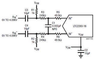
Thus, I'm thinking if it is a good practice to use AC coupling between them. I found several notes (see below for an example) mentioning this technique, and it seems like it is likely to work for ADS131M02 too. 
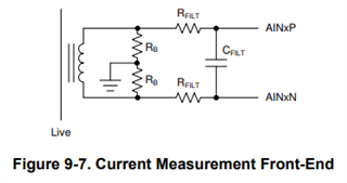
I also noticed that in ADS131M02's datasheet, there's a demonstration of measuring the current, where the common mode bias is set to AGND and the signal path is somewhat similar to AC coupling (by a transformer).

My questions are:

1. Can I use AC coupling in my design like what the first figure shows?

2. Can I simply set the Vcm = 0 (AGND) like what the second figure shows? As the ADC can only measure differential signal no higher than +-1.2v, I think this won't cause any trouble even at the lowest gain?

3. Should I tune the parameters of the anti-aliasing filter after AC coupling?
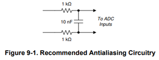
4. Any other tips or cautions when selecting the components' values? I saw something called pop noise from larger coupling caps, but I don't think it is as serious as I'm not going to read the results immediately.

Any help would be appreciated. Thanks in advance.

  • Hi Yucheng,

    Welcome to TI E2E forum.

    Can you please let me know what your actual signa from the op-amp (amplitude and common-mode voltage) and also the frequency of your signal are?

    The transformer in the circuit you highlighted is a current transformer that is commonly used to measure a current from in metering or grid application.

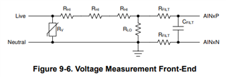
    ADS131M02 can be used to measure a true differential signal or a single-ended signal (AINxN is shorted to GND as shown in the figure 9-6 in the datasheet).

    BR,

    Dale

  • Hi Dale,

    Thank you for your info. The op-amp is configed as the differential buffer like the first stage of an instrumentation amp with a gain of 100 on each. So a 1mV diff signal will be amplified to 200mV in the output. My design needs to handle inputs from as low as 0.5uV to 6mV, so the output diff signal will be 100uV ~ 1.2V (maximum swing of ADS131M02)  at 10KHz. At such large swing and 3.3V VCC I can't find a good bias working for both devices by DC coupling. So I set the AC coupling caps to 1uF and bias resistors 10K to AGND and concatenate the anti-anliasing filter after that, and the simulation seems working, but I'm not sure if I have missed something.

    Best,

    YC

  • Hi YC,

    Thanks for sharing the information. ADS131M02 can measure a differential input signal up to -1.2V~1.2V, and also it can operate up to 64ksps data rate, so there is no issue for you to use this ADC to measure your signal, but you may have to consider the following specifications:

    • The higher data rate, the higher noise, for example, the noise will be 75.34uVrms on ADS131M02 when the data rate is 64ksps and Gain=1. The noise is much higher than your minimum signal 100uV on the ADC input. 
    • The offset error is 175uV typical on ADS131M02, the global-chop mode can be used to improve the offset and the noise but it will increase the settling time and limit the data rate of the ADC. A calibration can be considered as well.

    ADS131A02 is 2-ch simultaneous-sampling delta-sigma ADC that can support the data rate up to 128ksps, its noise is lower than ADS131M02 under the same conditions, 22.64uVrms at 64ksps data rate and Gain=1, an offset error calibration is needed. ADS131A02 supports a differential or single-ended input signal.

    I'm not sure whether a simultaneous-sampling ADC is definitely required in your design or not. TI has other precision ADC that has lower noise, but I would suggest you to take a look at ADS131A02 first.

    BR,

    Dale

  • Hi Dale,

    Thanks for the reply. I checked the specs of ADS131M02 and ADS131A02, please correct me if I'm wrong:

    1. ADS131A02 seems a bit pricy compared to ADS131M02. My SDR works only on digitally encoded signals other than analog audio, so I think the device isn't very sensitive to noise as long as SNR>=3dB.

    2. The datasheet of ADS131M02 (Vref 1.2V) states that for 64ksps and gain = 32 the effective resolution is 13.7 bits, so a 100uV diff signal will result in an effective readout of 100/(2*1.2*1e6/2^13.7/32) = 17.7, which seems to have enough space for detecting weak signals by digital filtering.

    3. The same formula applied to ADS131A02 (Vref 2.44V) yields 100/(2*2.44*1e6/2^15.71/4) = 4.4, otherwise an external precision Vref is required.

    3. I need to convert the RF mixer's analog IQ signal and reconstruct it in the discrete domain, so I think simultaneous sampling is necessary.

    Best,

    Yucheng

  • Hi Yucheng,

    I do not know what your calculation in 2 and 3 are, the effective resolution of the device is only related to the RMS noise, the reference voltage and the Gain. I would suggest you to get an EVM board and test it with your actual signal first to see if the ADC can meet your requirement.

    BR,

    Dale