This thread has been locked.

If you have a related question, please click the "Ask a related question" button in the top right corner. The newly created question will be automatically linked to this question.

ADS1299: schematic design and layout note

Part Number: ADS1299

Tool/software:

Hi,

Since this is our first time using the EEG ADS1299 chip,  we need more information on the precautions for circuit design and layout.

Excpet the ADS1299 website folder, is there have any ohter additional resources can share to us? Thanks!

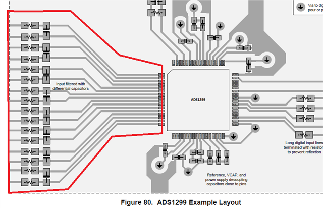
Could you please clarify whether the marked lines below require impedance matching? Additionally, does the entire ADS1299 circuit need to be designed with shielding?

Jeff

  • Hello Jeff,

    Thank you for your post.

    You should try to route the P and N channel input traces differentially, but the total impedance does not need to be tightly controlled. The overall impedance matching will be dominated by the passive component tolerances (namely the resistors and capacitors used for protection or antialiasing).

    The traces or ADS1299 itself does not necessarily require shielding. However, a solid ground plane below the device is recommended. 

    Regards,

    Ryan

  • Hi Ryan,

    Got it and thank you.

    Jeff