Other Parts Discussed in Thread: AMC131M03
Tool/software:
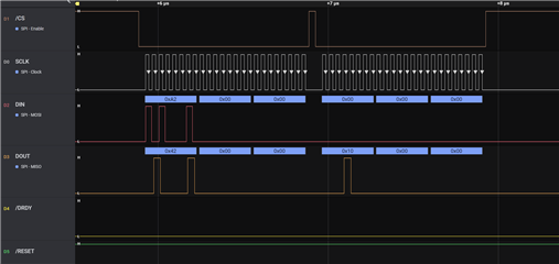
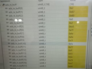
Hi im using ADS131M04, im trying to communicate with the ic, im reading the default registers value, but data is incorrect.in the just trying to read the mode register default value.
uint16_t ADS_ReadRegister(uint8_t reg_addr)
{
uint8_t tx_buf[3] = { 0 };
uint8_t rx_buf[3] = { 0 };
// RREG command format: 001a aaaa annn nnnn → 0x20 | (addr << 1)
uint16_t opcodes;
opcodes = OPCODE_RREG | (((uint16_t) reg_addr) << 7);
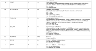
tx_buf[0] = (uint8_t)((opcodes >> 8) & 0x00FF);
tx_buf[1] = (uint8_t)(opcodes & 0x00FF);
tx_buf[2] = 0;
HAL_SPI_TransmitReceive_DMA(&hspi3, tx_buf, rx_buf, 3);
return ((uint16_t)rx_buf[0] << 8) | ((uint16_t)rx_buf[1]);
}
void ADS_WriteRegister(uint8_t reg_addr, uint16_t data)
{
uint8_t tx_buf[6] = {0};
uint8_t rx_buf[6] = {0};;
uint16_t opcodes[1];
opcodes[0] = OPCODE_WREG | (((uint16_t) reg_addr) << 7);
// WREG command format: 011a aaaa annn nnnn → 0x60 | (addr << 1)
tx_buf[0] = (uint8_t)((opcodes[0] >> 8) & 0x00FF);
tx_buf[1] = (uint8_t)(opcodes[0] & 0x00FF);
tx_buf[2] = 0x0;
tx_buf[3] = (uint8_t)(data >> 8) & 0x00FF;
tx_buf[4] = (uint8_t)data & 0x00FF;
tx_buf[5] = 0x0;;
HAL_GPIO_WritePin(CS2_GPIO_Port, CS2_Pin, GPIO_PIN_RESET);
HAL_SPI_TransmitReceive_DMA(&hspi3, tx_buf, rx_buf, 6);
HAL_GPIO_WritePin(CS2_GPIO_Port, CS2_Pin, GPIO_PIN_SET);
return;
}
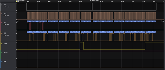
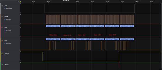
both the read and write or not working and onemore the ic is started giving the data continuosly example 4ksps for default mode value. im making chipselect low for continuously.
what to do any suggestion, is there frame format is correct or not. MY SPI CLK IS 10MHZ AND CLKIN IS 8MHZ