


Tool/software:
Hi TI's experts,
I am new to AFE4490. While reading its datasheet, I am little confused by the pin usage of SCLK and related read/write mode.
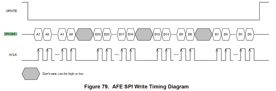
On the datasheet(SBAS602H –DECEMBER 2012–REVISED OCTOBER 2014), P52, it is written as "SCLK features a Schmitt-triggered input and clocks data out on SPISOMI."
On page 85, the schematic diagram 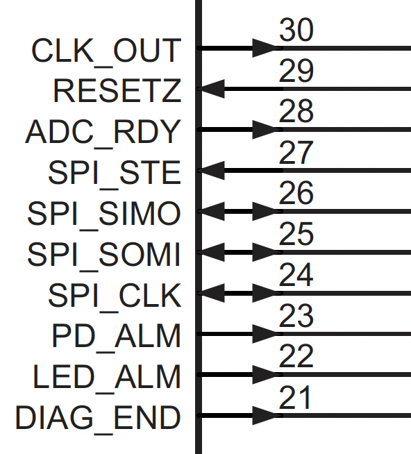 ,
,
the SCLK is marked as a bi-directional function.
In its writing mode, the connected MCU makes the SPISTE low and sends the SCLK with the synchronized data bits on SPISIMO pin. Here, the MCU is SCLK sender and AFE4490 is the SCLK receiver.
BTW, can the MCU ignore those discontinues between A0-bit and D32-bit, between D16-bit and D15-bit, and between D8-bit and D7-bit (depicted in Figure 79 on P52), and send SCLK continuously and uniformly with entire 32 bits, from A7 to D0?
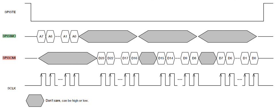
In its reading mode, need the MCU swap its role of SCLK pin to be a receiver after the first 8 bits of address A7-to-A0?If not, may the MCU keep sending SCLK and check the state of SPISOMI pin? Again, may the MCU ignore those discontinues depicted in Figure 80.
If the MCU has to swap its SCLK role during a read session or a Multiple Data Reads and Writes session, what MCU would TI recommend?
Please help me in understanding AFE4490's datasheet correctly and thank you!
Best Regards!
Wallace