


Other Parts Discussed in Thread: ADS8688
Tool/software:
Dear colleagues,
in our design we are using a ADS8668 ADC to measure the DC offset at the input of an amplifier. Typical values we expect range from -1 V to + 1V.
Unfortunately, an error was introduced in the design, so that, for inputs 4, 5, 6, and 7 the signal to be sampled is connected to AIN_nGND, while AIN_nP is connected to ground.
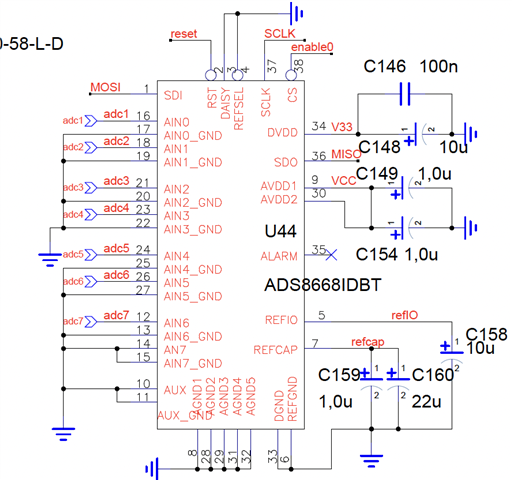
As you see in the above schematic, AIN4, the input signal pin for ADC 4, is marked as pin number. 24, and the corresponding GND pin is marked as pin number 25. These are inverted (issue was introduced when the ad-hoc symbol for ADS8668 was created by scratch for this project). Same issue for channel 5.
Indeed, when reading data from the ADC, the obtained value is exactly the real one, but inverted (real one was measured on the circuit with a multimeter). This can be easily accounted for in the software.
However, I am wondering if this configuration may damage the ADC. Reading from the ADS8668 datasheet, I see the following (Sec. 8.3.1, pag 23):
The devices allow a ±0.1-V range on the AIN_nGND pin for all analog input channels.
This is also reported in tab. 7.5, "electrical characteristics"
At the same time, in the absolute maximum ratings table (7.1) I see that the min/max values for the difference between AIN_nGND to GND is -11 V/ +11 V or -20 V / + 20 V depending on the AVDD configuration.
So, to summarize, in my application I am well within the maximum ratings, and apparently the readout works properly, with the factor "-1" due to input signals inversion.
May I ask you if there is any clear issue with this (erroneous) design?
Thanks,
Bests,
Andrea Celentano
