This thread has been locked.

If you have a related question, please click the "Ask a related question" button in the top right corner. The newly created question will be automatically linked to this question.

ADS1256: Using F280049C to read ADS1256 registers

Part Number: ADS1256
Other Parts Discussed in Thread: TMS320F280049

Tool/software:

I’m working with a TMS320F280049 to interface with an ADS1256. I’ve configured the F280049’s SPI for Mode 1 at 1 MHz, without using FIFO or interrupts, but I’m unable to read any ADS1256 registers correctly—even though my logic analyzer traces look reasonable, the ADC keeps returning spurious data. Below are my initialization code and the function I’m using to read a register:

void ADS1256_writeRegister(uint8_t reg, uint8_t value) {
 CS_LOW();
 while (GPIO_readPin(ADS1256_DRDY_GPIO))
 ;
 SPI_writeByte(ADS1256_CMD_WREG | (reg & 0x0F));

 SPI_writeByte(0x00); // write one register
 SPI_writeByte(value);
 CS_HIGH();
}

static void ADS1256_sendCmd(uint8_t cmd) {
 CS_LOW();
 SPI_writeByte(cmd);
 CS_HIGH();
}

void ADS1256_init(void) {
 while (GPIO_readPin(ADS1256_DRDY_GPIO))
 ;
 CS_LOW();
 SPI_writeByte(ADS1256_CMD_SELFCAL);
 while (GPIO_readPin(ADS1256_DRDY_GPIO))
 ;
 CS_HIGH();

 ADS1256_writeRegister(ADS1256_STATUS, 0x06);

 ADS1256_writeRegister(ADS1256_ADCON, ADS1256_PGA_GAIN_1);
 ADS1256_writeRegister(ADS1256_DRATE, 0x23);
 ADS1256_writeRegister(ADS1256_IO, 0x00);

 while (GPIO_readPin(ADS1256_DRDY_GPIO))
 ;
 CS_LOW();
 SPI_writeByte(ADS1256_CMD_SELFCAL);
 while (GPIO_readPin(ADS1256_DRDY_GPIO))
 ;
 CS_HIGH();
}

uint8_t ADS1256_readRegister(uint8_t reg) {
 uint8_t val;

 ADS1256_sendCmd(ADS1256_CMD_SDATAC);
 
 while (GPIO_readPin(ADS1256_DRDY_GPIO))
 ;
 CS_LOW();

 SPI_writeByte(ADS1256_CMD_RREG | (reg & 0x0F));
 SPI_writeByte(0x01); // read one register

 DEVICE_DELAY_US(50);
 // val = SPI_receiveByte(ADS1256_SPI_BASE, 0x00);
 // val = SPI_receiveByte(ADS1256_SPI_BASE, 0x00);

 CS_HIGH();
 return val;
}

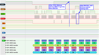
I ran the ADS1256_readRegister() function inside a loop, and the results are shown in the figure below:


In the figure above, the MISO data stream is irregular. Instead of the two expected bytes from the registers I’m reading, the output appears garbled.

Zooming in on the capture, the SPI commands and data bytes sent by the master look as expected, but the data coming back from the ADS1256 remains garbled: two valid register bytes never appear on MISO.


Thank you in advance for assistance!

  • Hello Chen,

    The ADS1256 transmits data on the rising edge of SCLK and captures data on the falling edge of SCLK.  According to the F280049 user's guide, you need to select 'Rising edge without delay', or SPI mode 00.  Using SPI mode 1 will cause setup and hold time violations.

    Also, in order to read from a single register, the SPI frame needs to be 3 bytes long.  During this time, the /CS line must remain low, or the SPI port will be reset and the read register command will not be executed.  Figure 34 shows the proper command sequence to read 2 registers, starting with the MUX.

    First, send command 0x1101h, delay t6=50 CLK periods.  Assuming you are using an 8MHz clock, then you need to delay for a minimum t6=50*125ns=6.25us.  Then, read the MUX and ADCON registers by sending 16 SCLKs.  The ADS1256 will transmit data on the rising edge of SCLK, and the F280049 should capture the data on the SCLK falling edge.

    Regards,
    Keith Nicholas
    Precision ADC Applications

  • Hi, thanks for your help! I’ve successfully read the ADS1256 registers. Now I’m trying to read the conversion data: I’ve selected channel 0 and sent the corresponding command and register settings. The values I’m seeing look plausible, but shouldn’t the ADC only output three bytes immediately after the master issues the 0x03 (RDATA) command?

    In the capture above, I see six additional bytes transmitted before the three expected data bytes (0x28 0x89 0xF8). What are those extra bytes, and do they contain any useful information?

  • Hello Chen,

    You need to add some additional delays.

    After sending the SYNC and WAKEUP commands, you need to wait for DRDY to go low, then send the RDATAC command.

    After sending the RDATAC command, you need to wait at least 6.5us (t6=50*tCLK); you are only waiting about 4us in this case.

    Details can be found here:

    You are sending a total of 5 SPI frames.  The first frame (WREG to set the MUX input), the ADC is providing the last output data of 0x2889f8h.  Since there are no new conversion results, you are getting the same data repeated.  The next 3 frames are only 8b, so you only get 0x28h, but then the last frame, you are clocking 24b, which is providing the full 24b data again.

    Regards,
    Keith