This thread has been locked.

If you have a related question, please click the "Ask a related question" button in the top right corner. The newly created question will be automatically linked to this question.

ADS1299-4: PCB layout support

Part Number: ADS1299-4

Tool/software:

Hi everyone.
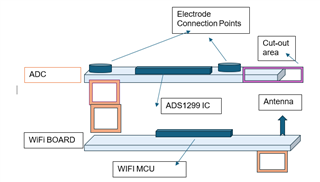
Im making a board with ADC ADS1299-4 and controller integrated WIFI functions.
One board for ADC and other board for WIFI controller, 2 boards were connected by B2B connector (height btw B2B conn is 2.5mm).
How are the best option for ADC parts placement to improve/cancel a noise/interference ?

*Opt1: ADS1299-4 placed on bottom layer board, near WIFI MCU

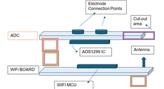
*Opt2: ADS placed on top layer board, near electrode

Thank you.

  • Hello Zuan,

    Option 2 makes the most sense, in my opinion. The AD1299 should be placed in close proximity to the electrode inputs. Having these components on the top of Board 1 will allow the bottom layer(s) to act as a ground shielding and reduce any potential noise coupling from the WIFI/MCU board.

    Regards,

    Ryan