This thread has been locked.

If you have a related question, please click the "Ask a related question" button in the top right corner. The newly created question will be automatically linked to this question.

DAC8551: DAC8551 Output Issue When VDD = VREF = 5V and VFB = VOUT

Other Parts Discussed in Thread: DAC8551

Hello TI Support,

I'm using the DAC8551 in an application where:

  • VREF = 5 V

  • VDD= 5 V

  • VFB is externally connected to VOUT, as recommended for voltage output mode.

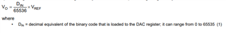
Based on the datasheet (section 7.3.1.2), the internal output amplifier has a 2× gain, so the expected output is:

VOUT = 2 ×( DIN  / 65536) × VREF

However, I observe the following behavior:

  • For DIN ≤ 32767, VOUT behaves as expected.

  • For DIN > 32767, VOUT suddenly drops to 0 V or becomes unstable.


My Questions:

  1. Is this behavior expected due to the fact that VOUT attempts to exceed VDD (i.e., >5 V) because of the 2× gain?

  2. If so, is reducing VREF to 2.5 V the recommended solution to safely use the full DAC input range?

  3. Is there any internal clamping or protection behavior that causes the output to go low instead of just saturating at VDD?

  4. Are there any stability considerations with VFB = VOUT that I should account for?

Any clarification on this would be appreciated.

Thanks in advance!

Best regards,
Danidu.

  • Hi Danidu, 

    The output has a 2x gain, but this is because the internal DAC resistor divider has a divide by 2. So the full-scale output range of a 5V reference should be 0 to 5V.

    For DIN < 32767, what output range do you see?

    Do you have any load on the output? Capacitive loads can cause instability to buffered DACs, but it does not sound like this is what you are seeing. Can you elaborate more on what happens after code 32767? 

    Best,

    Katlynne Jones

  • Hi Katlynne,

    for DIN < 32767, my output range is from 0V to 5V.
    Output is connected to an opamp (acting as a subtractor).
    After code 32767, the output seems to be giving random values (mostly 0V).
    Is it possible that the IC got damaged somehow? 

    Best,
    Danidu. 

  • Hi Danidu, 

    I wouldn't expect this behavior from a damaged device either, but it's possible. Do you have any devices or boards to do an A-B-A swap with. I assume the device behaves the same even after a power cycle. Are you measuring at the output of the DAC or output of the op amp? 

    Are you able to try a smaller reference like 2.5V and check the behavior? 

    Best,

    Katlynne Jones

  • Hi Katlynne,

    Currently it is soldered to a PCB, so there is no way for me to change the reference voltage.
    I am measuring from the output of the DAC.
    I have some spare ICs, i will replace the current one and test it again.

    Thank you very much for your help, i wanted to clarify how the Vout is calculated. 

    Best,
    Danidu.

  • Hi Danidu, 

    Yes, the full-scale range should be 0 to VREF with VOUT = VREF * DIN /2^16. 

    Let me know if you are still facing an issue after trying a new IC. 

    Best,

    Katlynne Jones

  • Hi Katlynne,

    The DAC is working as expected, the problem was I using SPI Mode 0 that's why it was showing that weird behavior.
    When I changed it to SPI Mode 1( since the DAC reads data on the falling edge of the clock (CPHA=1)) it worked properly.

    Sorry for troubling you for my silly mistake.
    Thanks again for helping me out!

    Best,
    Danidu.