This thread has been locked.

If you have a related question, please click the "Ask a related question" button in the top right corner. The newly created question will be automatically linked to this question.

ADS131M04: Question about the schematic design

Part Number: ADS131M04

Tool/software:

Hello everyone. I'm using an ADS131M04 in a project, but I can't get it to work.

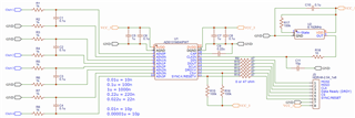
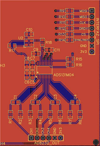
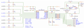
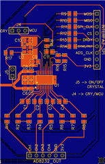
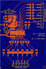
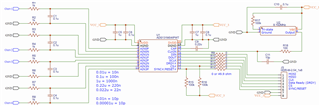
I'm trying to test it with some Arduino code I found on GitHub that supposedly works.
So, I'm going to assume the programming isn't the problem. So, I'd like to ask if my design is correct. I built it based on the information in the datasheet and other designs I found online, but I can't get it to work.

Can you tell me if my design is correct?


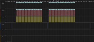
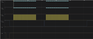
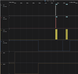
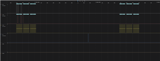
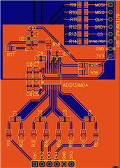
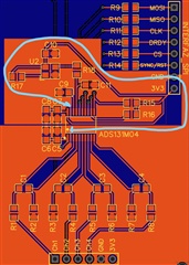
Also, i add a logic test. Here, i was trying to read the ID register (00h), I expected to see the values ​​of bits 15:8, that is, the value (24h), but I get this. Also, I find it very strange that on the MISO line, I see pulses similar to those on the CLK line, but I already checked that they are not connected to each other. In fact, when I send the first bits, the values ​​between the MISO and CLK lines are different. I really don't know why these pulses appear on the MISO line.


  • While I wait for a response from a professional, I'll post progress in case it might be helpful to anyone. I was able to resolve the pulses on the MISO line by placing a 10k resistor between the MISO line and GND. However, the ADS131M04 still doesn't respond. Here's an image of the last logic test I performed. I also tried another microcontroller, but the ADS131M04 still doesn't work.


    I think it could be one of three things: The circuit is poorly designed, or it's not soldered properly.
    But I've checked several times that the lines are soldered correctly and that there are no short circuits. Which brings me to the last option: I was unlucky that the ADS131M0 I'm using is defective, but I can't be sure either.

    I'll keep trying more things.


  • Hi Edgar Eduardo Arellano Zuvieta,

    Thank you for your update. Your query was posted in the weekend.

    Your schematic looks goo and I did not see any issue. Using a small value series resistor (e.g. 49.9ohm) on the digital bus will be better than a 0ohm resistor.

    Using a pull-down resistor on the MISO is not necessary, it can indicate some problems on the PCB layout if the pulses were disappeared with the resistor.

    After the ADC is powered up, can you see continuous pulses on the /DRDY from the ADC? not need to program any registers.

    What are your SCLK frequency and configuration? the configuration on your microcontroller should be CPOL=0, CPHA=1.

    You can send the whole frame to read a register, or just a timing like this:

    RREG_reading the GAIN register (0x4 address)

    BR,

    Dale

  • Hi Dale.
    Before, Thank you for your time. 


    Now, firts of all, i changed the IC for a new one. And i got better results. I think the previous one was damaged.

    Anyway, I'm going to answer you in order:

    1. With this new IC, I no longer have any problems with the MISO line. So i was able to remove the pull-down resistor.

    2. 
    When I power up the circuit, I don't see any pulses from the /DRDY. I only see a long pulse when I perform a reset using the RESET/SYNC pin. Just like in the image.


    3. I think I have the recommended configuration. I mean, I have the SPI peripheral set to 8MHz and in mode 1.

    4. If I send RREG along with address 0x04, that is, 0x42 as you show in your image, I get the following:


    Sorry for the long time delays, this is how the Raspberry Pi Zero 2w handles it. Could this be a problem?


    Thank you, and I look forward to your response.
    Best regards!
  • Hi Edgar Eduardo Arellano Zuvieta,

    Thank you for your reply and update.

    2. Can you share your schematic and also let me know your connections between the ADC and the microcontroller?

    4. In my timing example, I had written 0x1000 into the GAIN1 register before reading it. By default, the GAIN1 on M04 ADC has 0x0000 register value, so maybe you can read other registers that do not have 0x0000 default value, for example, MODE or CLOCK register.

    The duty cycle of your SCLK is not 50-50%, you may have to check your clock source.

    BR,

    Dale

  • Hi Dale!

    2. Of course. In the first image, I show you the design I created. And in the second, the PCB layout, in case it helps.


    In my design, I tried to separate the analog and digital grounds, which is why you see a line in the middle of the circuit. The top layer is ground. The bottom layer is for VDD. If you have any recommendations on the PCB design, I would appreciate it. I'm sharing my full PCB design with you in case it helps you in any way. The top layer is shown on the right, and the bottom layer is shown on the left.


    4. I was finally able to read the ID register. But I found something that gave me goosebumps. I don't understand it, but apparently my circuit only works without connecting VDD from the microcontroller to the ADS. It's very strange, but I can read the registers and channel values ​​without connecting to VDD. I understand that the ADS draws power from the SPI line, and this happens on two different microcontrollers, so I assume the problem isn't with the microcontrollers, but the problem may be with the board or the ADS. Specifically, it draws power from the CS pin and the RESET pin. I checked this with a multimeter.

    I really don't know what to make of this. I think I'll buy other ADSs from a more reliable store. I'd just like you to confirm that the PCB design is correct or what changes you would recommend.

    Best regards!

    Edgar.

  • Hi Edgar,

    Your schematic looks good to me, but the biggest problem on your PCB layout is, the ground connection and the return path for current is too long as you can see the blue line in the following image. Splitting ground is not necessary if it is not required. A solid and dedicated ground plane is usually recommended for both AGND and DGND. If splitting ground is needed, a short point should be placed close to the ADC.

    BR,

    Dale

  • Hi Dale.

    Thank you for your recomendations. I changed my design to the following. What do you think? Basically, the entire top layer is GND, while the entire bottom layer is VDD. Do you think this is correct?


    Best regards!
    Edgar.

  • Hi Edgar,

    1. Place the components close to the ADC especially the capacitors

    2. It's not necessary to use an entire layer for the power supply. You can use the bottom layer for the GND, then use vias.

    3. You can use a wide trace for the power supply. The power supply should go to the coupling capacitors first then go to the AVDD or DVDD of the ADC for the best coupling result. See the via that is close to C5 and C6 you are using for AVDD, that is not a good layout design.

    BR,

    Dale

  • Hi Dale.

    Thanks you for your recomendations. I made the adjustments based on your recommendations, and even added a couple of jumpers to change the ADS131M04's clock source. I'm showing you the schematic in case you have any recommendations.


    For the PCB, I removed the VDD layer as you suggested and implemented power supply traces. I also made sure the power supply passes through the capacitors first and generally moved the components closer to the ADS. I also left the bottom layer as ground and only used vias to connect the ADS pins and some components to ground. I'm also showing you an image in case you have any recommendations. In this case, the red areas are copper connected by a via to the bottom ground layer.

  • Hi Edgar,

    The new layout looks better, but I still have suggestions for you:

    • You could move R18 and C11 to have a little bit more space so that the traces of all digital signals can be placed on the top layer only, not need to use so many vias for these digital SPI signals.
    • You could move J4 to make the trace of CLK is shorter and no need to use a via for CLK signal. You could use 0ohm resistors instead of a header if needed.
    • Use a dedicated via for ground connection on R6,R7,R2 and R3).
    • No 90 degree turning trace, see the trace to R8.
    • The resistors from R1 to R8 can be placed closer to make the traces a little shorter, this is optional.

    BR,

    Dale

  • Hi Dale. 

    I made the changes you recommended. I'm not sure I understood your second recommendation, but I still removed the via that was in the CLK trace. What do you think of the new design?

  • Hi Edgar,

    I apologized for the late response. This Monday was a holiday.

    This layout looks better. What I said was, J4 could be placed to the right side of U2 and close to the ADC so the trace could be shorter.

    You can use more vias to connect the ground plane on the top and bottom layer. 

    BR,

    Dale

  • Hi Dale!
    I also apologize for the late response.

    Thank you for your all recomendations. I think it's enough to get better results than my old PCB.
    With this, I will conclude the post.