Other Parts Discussed in Thread: ADS125H02, , ADS125H02EVM
Tool/software:
Hi,
I am currently working on a design that uses an ADS124S08 and ADS125H02 to take ADC readings.
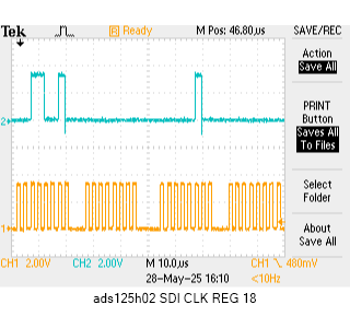
SPI is set to mode 1, the speed is set to 400kHz and they share the SCLK, SDI and SDO lines.
I have based the code on the library on github and modified it to work with the SPI library of the PIC32MM0256GPM064
I have checked the voltages on the AVDD, IODD, and DVDD pins of the ADS124S08 and they are 5V, 3.3V and 3.3V respectively. Same for the ADS125H02 with HV_AVDD being 5V as well. all the VSS are connected to GND.
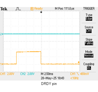
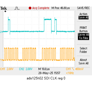
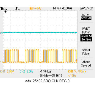
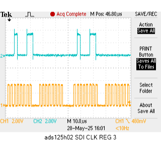
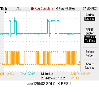
I tried to test the communication by polling registers 0x00 - 0x09 and the response I am getting is 0.
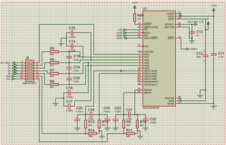
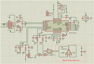
I am attaching the circuit diagram for both the devices, I saw missing connection between start pin to GND and have connected a wire physically. I plan to take single shot measurements and start conversion via commands. For the ADS125H02 I had to physically short it to ground as well as it is missing in the circuit diagram.
I am also including the library files for both the devices.
Could you please help me identify what I am doing incorrectly.
/**
 *
 * @file ads124s08.c
 *
 * @brief  ADS124S08 Low level routines using TI Drivers
 *
 * @copyright Copyright (C) 2019-22 Texas Instruments Incorporated - http://www.ti.com/
 * All rights reserved.
 *
 *  Redistribution and use in source and binary forms, with or without
 *  modification, are permitted provided that the following conditions
 *  are met:
 *
 *    Redistributions of source code must retain the above copyright
 *    notice, this list of conditions and the following disclaimer.
 *
 *    Redistributions in binary form must reproduce the above copyright
 *    notice, this list of conditions and the following disclaimer in the
 *    documentation and/or other materials provided with the
 *    distribution.
 *
 *    Neither the name of Texas Instruments Incorporated nor the names of
 *    its contributors may be used to endorse or promote products derived
 *    from this software without specific prior written permission.
 *
 *  THIS SOFTWARE IS PROVIDED BY THE COPYRIGHT HOLDERS AND CONTRIBUTORS
 *  "AS IS" AND ANY EXPRESS OR IMPLIED WARRANTIES, INCLUDING, BUT NOT
 *  LIMITED TO, THE IMPLIED WARRANTIES OF MERCHANTABILITY AND FITNESS FOR
 *  A PARTICULAR PURPOSE ARE DISCLAIMED. IN NO EVENT SHALL THE COPYRIGHT
 *  OWNER OR CONTRIBUTORS BE LIABLE FOR ANY DIRECT, INDIRECT, INCIDENTAL,
 *  SPECIAL, EXEMPLARY, OR CONSEQUENTIAL DAMAGES (INCLUDING, BUT NOT
 *  LIMITED TO, PROCUREMENT OF SUBSTITUTE GOODS OR SERVICES; LOSS OF USE,
 *  DATA, OR PROFITS; OR BUSINESS INTERRUPTION) HOWEVER CAUSED AND ON ANY
 *  THEORY OF LIABILITY, WHETHER IN CONTRACT, STRICT LIABILITY, OR TORT
 *  (INCLUDING NEGLIGENCE OR OTHERWISE) ARISING IN ANY WAY OUT OF THE USE
 *  OF THIS SOFTWARE, EVEN IF ADVISED OF THE POSSIBILITY OF SUCH DAMAGE.
 *
 */
#include <stdbool.h>
#include <musl/stdint.h>
#include <musl/math.h>
#include <musl/assert.h>

//#include "hal.h"//
#include "mcc_generated_files/drivers/spi_master.h"
#include "mcc_generated_files/delay.h"
#include "ADS124S08.h"
#include "crc.h"
#include "mcc_generated_files/pin_manager.h"
#include "LCD2.h"
#include "print_lcd.h"

//****************************************************************************
//
// Internal variables
//
//****************************************************************************

/* Internal register map array (to recall current configuration) */
static uint8_t registerMap[NUM_REGISTERS];

//****************************************************************************
//
// Functions
//
//****************************************************************************

/************************************************************************************//**
 *
 * @brief getRegisterValue()
 *          Getter function to access the registerMap array outside of this module
 *
 * @param[in]	address	The 8-bit register address
 *
 * @return 		The 8-bit register value
 */
uint8_t getRegisterValue( uint8_t address )
{
    assert( address < NUM_REGISTERS );
    return registerMap[address];
}

/************************************************************************************//**
 *
 * @brief adcStartupRoutine()
 *          Startup function to be called before communicating with the ADC
 *
 * @param[in]   *spiHdl    SPI_Handle pointer for TI Drivers
 *
 * @return      true for successful initialization
 *              false for unsuccessful initialization
 */
 bool adcStartupRoutine( void )
{
    uint8_t initRegisterMap[NUM_REGISTERS] = { 0 };
    uint8_t status, i;

    // Provide additional delay time for power supply settling
    DELAY_microseconds( DELAY_2p2MS );

    // Toggle nRESET pin to assure default register settings.
    //toggleRESET();
    resetADC();

    // Must wait 4096 tCLK after reset
    DELAY_microseconds( DELAY_4096TCLK );

    status = readSingleRegister( REG_ADDR_STATUS );
    if ( (status & ADS_nRDY_MASK) ) {
        return( false );                      // Device not ready
    }

    // Ensure internal register array is initialized
    restoreRegisterDefaults();

    // Configure initial device register settings here
    writeSingleRegister( REG_ADDR_STATUS, 0x00 );    // Reset POR event

    // Create temporary array based on desired configuration
    for( i = 0 ; i < NUM_REGISTERS ; i++) {
        initRegisterMap[i] = registerMap[i];
    }

    // Read back all registers, except for status register.
    readMultipleRegisters( REG_ADDR_ID, NUM_REGISTERS );
    for ( i = REG_ADDR_STATUS; i < REG_ADDR_SYS - REG_ADDR_STATUS + 1; i++ ) {
        if ( i == REG_ADDR_STATUS )
            continue;
        if ( initRegisterMap[i] != registerMap[i] )
            return( false );
    }
    return( true );
}

/************************************************************************************//**
 *
 * @brief readSingleRegister()
 *          Reads contents of a single register at the specified address
 *
 * @param[in]   spiHdl  SPI_Handle from TI Drivers
 * @param[in]	address Address of the register to be read
 *
 * @return 		8-bit register contents
 */
uint8_t readSingleRegister( uint8_t address )
{
    /* Initialize arrays */
    uint8_t DataTx[COMMAND_LENGTH + 1] = { OPCODE_RREG | (address & OPCODE_RWREG_MASK), 0, 0 };
    uint8_t DataRx[COMMAND_LENGTH + 1] = { 0, 0, 0 };


    /* Check that the register address is in range */
    assert( address < NUM_REGISTERS );
    memcpy(DataRx,DataTx,COMMAND_LENGTH+1);
    /* Build TX array and send it */
    CS2_SetLow();
//    DELAY_microseconds(1);
    //spiSendReceiveArrays( DataTx, DataRx, COMMAND_LENGTH + 1);
    spi2_exchangeBlock(&DataRx,COMMAND_LENGTH + 1);
    CS2_SetHigh();

    /* Update register array and return read result*/
    registerMap[address] = DataRx[COMMAND_LENGTH];
    return DataRx[COMMAND_LENGTH];
}

/************************************************************************************//**
 *
 * @brief readMultipleRegisters()
 *          Reads a group of registers starting at the specified address
 *          NOTE: Use getRegisterValue() to retrieve the read values
 *
 * @param[in]   spiHdl          SPI_Handle from TI Drivers
 * @param[in]	startAddress	Register address to start reading
 * @param[in]	count 			Number of registers to read
 *
 * @return 		None
 */
void readMultipleRegisters( uint8_t startAddress, uint8_t count )
{
    uint8_t DataTx[COMMAND_LENGTH + NUM_REGISTERS] = { 0 };
    uint8_t DataRx[COMMAND_LENGTH + NUM_REGISTERS] = { 0 };
    uint8_t i;

    /* Check that the register address and count are in range */
    assert( startAddress + count <= NUM_REGISTERS );

    // Read register data bytes
    DataTx[0] = OPCODE_RREG | (startAddress & OPCODE_RWREG_MASK);
    DataTx[1] = count - 1;
    memcpy(DataRx,DataTx,COMMAND_LENGTH+count);
    CS2_SetLow();
////    DELAY_microseconds(1);
    //spiSendReceiveArrays( DataTx, DataRx, COMMAND_LENGTH + count);
    spi2_exchangeBlock(&DataRx,COMMAND_LENGTH + count);
    CS2_SetHigh();

    for ( i = 0; i < count; i++ ) {
        // Store received register data into internal registerMap copy
        registerMap[i+startAddress] = DataRx[COMMAND_LENGTH + i];
    }
}

/************************************************************************************//**
 *
 * @brief writeSingleRegister()
 *          Write data to a single register at the specified address
 *
 * @param[in]   spiHdl      SPI_Handle from TI Drivers
 * @param[in]	address 	Register address to write
 * @param[in]	data 		8-bit data to write
 *
 * @return 		None
 */
void writeSingleRegister( uint8_t address, uint8_t data )
{
    /* Initialize arrays */
    uint8_t DataTx[COMMAND_LENGTH + 1] = { OPCODE_WREG | (address & OPCODE_RWREG_MASK), 0, data};
    uint8_t DataRx[COMMAND_LENGTH + 1] = { 0 };

    /* Check that the register address is in range */
    assert( address < NUM_REGISTERS );
    //memcpy(DataRx,DataTx,COMMAND_LENGTH+1);
    /* Build TX array and send it */
    CS2_SetLow();
//    DELAY_microseconds(1);
    //spiSendReceiveArrays( DataTx, DataRx, COMMAND_LENGTH + 1 );
    //spi2_exchangeBlock(&DataRx,COMMAND_LENGTH + 1);
    for(int rx = 0; rx < (COMMAND_LENGTH+1);rx++){
        DataRx[rx]= spi2_exchangeByte(DataTx[rx]);
    }
    CS2_SetHigh();
//    LCD_add(0x00);
//    printf("%02X %02X %02X",DataTx[0],DataTx[1],DataTx[2]);

    /* Update register array */
    registerMap[address] = DataTx[COMMAND_LENGTH];
}

/************************************************************************************//**
 *
 * @brief writeMultipleRegisters()
 *          Write data to a group of registers
 *          NOTES: Use getRegisterValue() to retrieve the written values.
 *          Registers should be re-read after a write operation to ensure proper configuration.
 *
 * @param[in]   spiHdl          SPI_Handle from TI Drivers
 * @param[in]	startAddress 	Register address to start writing
 * @param[in]	count 			Number of registers to write
 * @param[in]	regData			Array that holds the data to write, where element zero
 *      						is the data to write to the starting address.
 *
 * @return 		None
 */
void writeMultipleRegisters( uint8_t startAddress, uint8_t count, uint8_t regData[] )
{
    uint8_t DataTx[COMMAND_LENGTH + NUM_REGISTERS] = { 0 };
    uint8_t DataRx[COMMAND_LENGTH + NUM_REGISTERS] = { 0 };
    uint8_t i, j = 0;

    /* Check that the register address and count are in range */
    assert( startAddress + count <= NUM_REGISTERS );

    /* Check that regData is not a NULL pointer */
    assert( regData );

    DataTx[0] = OPCODE_WREG | (startAddress & OPCODE_RWREG_MASK);
    DataTx[1] = count - 1;
    for ( i = startAddress; i < startAddress + count; i++ ) {
        DataTx[COMMAND_LENGTH + j++] = regData[i];
        registerMap[i] = regData[i];
    }
    memcpy(DataRx,DataTx,COMMAND_LENGTH+1);
    // SPI communication
    CS2_SetLow();
//    DELAY_microseconds(1);
    //spiSendReceiveArrays( DataTx, DataRx, COMMAND_LENGTH + count );
    spi2_exchangeBlock(&DataRx,COMMAND_LENGTH + count);
    CS2_SetHigh();

}

/************************************************************************************//**
 *
 * @brief sendCommand()
 *          Sends the specified SPI command to the ADC
 *
 * @param[in]   spiHdl      SPI_Handle from TI Drivers
 * @param[in]	op_code 	SPI command byte
 *
 * @return 		None
 */
void sendCommand( uint8_t op_code)
{
    /* Assert if this function is used to send any of the following commands */
    assert( OPCODE_RREG         != op_code );    /* Use "readSingleRegister()"  or "readMultipleRegisters()"  */
    assert( OPCODE_WREG         != op_code );    /* Use "writeSingleRegister()" or "writeMultipleRegisters()" */

    /* SPI communication */
    //spiSendReceiveByte( op_code );
    CS2_SetLow();
//    DELAY_microseconds(1);
    spi2_writeByte( op_code);
    CS2_SetHigh();

    // Check for RESET command
    if (OPCODE_RESET == op_code)
    {
        // Must wait 4096 tCLK after reset
        DELAY_microseconds( DELAY_4096TCLK );

        /* Update register array to keep software in sync with device */
        restoreRegisterDefaults();
    }
}

/************************************************************************************//**
 *
 * @brief startConversions()
 *        	Wakes the device from power-down and starts continuous conversions
 *            by setting START pin high or sending START Command
 *
 * @param[in]   spiHdl      SPI_Handle from TI Drivers
 *
 * @return 		None
 */
void startConversions( void )
{
	// Wakeup device if in POWERDOWN
    //sendWakeup( );
//    spi2_writeByte(OPCODE_WAKEUP);
    sendCommand(OPCODE_WAKEUP);

//#ifdef START_PIN_CONTROLLED     // If defined in ADS124S08.h
     /* Begin continuous conversions */
//    setSTART( HIGH );
//#else
    //sendSTART( );
//    CS2_SetLow();
//    DELAY_microseconds(1);
//    spi2_writeByte(OPCODE_START);
//    CS2_SetHigh();
    sendCommand(OPCODE_START);
//#endif
}

/************************************************************************************//**
 *
 * @brief stopConversions()
 *          Stops continuous conversions by setting START pin low or sending STOP Command
 *
 * @param[in]   spiHdl      SPI_Handle from TI Drivers
 *
 * @return      None
 */
void stopConversions( void )
{
     /* Stop continuous conversions */
//#ifdef START_PIN_CONTROLLED     // If defined in ADS124S08.h
//    setSTART( LOW );
//#else
    //sendSTOP();
//    CS2_SetLow();
//    DELAY_microseconds(1);
//    spi2_writeByte(OPCODE_STOP);
//    CS2_SetHigh();
    sendCommand(OPCODE_STOP);
//#endif
}

/************************************************************************************//**
 *
 * @brief resetADC()
 *          Resets ADC by setting RESET pin low or sending RESET Command
 *
 * @param[in]   spiHdl      SPI_Handle from TI Drivers
 *
 * @return      None
 */
void resetADC( void )
{
     /* Reset ADC */
//#ifdef RESET_PIN_CONTROLLED     // If defined in ADS124S08.h
    //toggleRESET();
//#else
    //sendRESET( );
    sendCommand(OPCODE_RESET);
//#endif
    // Must wait 4096 tCLK after reset
    DELAY_microseconds( DELAY_4096TCLK );

    // Update the local copy to say in sync
    restoreRegisterDefaults();
}

/************************************************************************************//**
 *
 * @brief readConvertedData()
 *          Sends the read command and retrieves STATUS (if enabled) and data
 *          NOTE: Call this function after /DRDY goes low and specify the
 *          the number of bytes to read and the starting position of data
 *
 * @param[in]   spiHdl      SPI_Handle from TI Drivers
 * @param[in]	status[] 	Pointer to location where STATUS byte will be stored
 * @param[in]	mode 		Direct or Command read mode
 *
 * @return 		32-bit sign-extended conversion result (data only)
 */
int32_t readConvertedData( uint8_t status[], readMode mode )
{
    uint8_t DataTx[RDATA_COMMAND_LENGTH + STATUS_LENGTH + DATA_LENGTH + CRC_LENGTH] = { 0 };    // Initialize all array elements to 0
    uint8_t DataRx[RDATA_COMMAND_LENGTH + STATUS_LENGTH + DATA_LENGTH + CRC_LENGTH] = { 0 };
    uint8_t byteLength;
    uint8_t dataPosition;
    uint8_t byte_options;
    uint8_t data[5];
    bool    status_byte_enabled = 0;
	int32_t signByte, upperByte, middleByte, lowerByte;

    // Status Byte is sent if SENDSTAT bit of SYS register is set
    byte_options = IS_SENDSTAT_SET << 1 | IS_CRC_SET;
    switch ( byte_options ) {
    	case 0:							// No STATUS and no CRC
			byteLength   = DATA_LENGTH;
			dataPosition = 0;
    		break;
    	case 1:							// No STATUS and CRC
    		byteLength 	 = DATA_LENGTH + CRC_LENGTH;
			dataPosition = 0;
   			break;
    	case 2:							// STATUS and no CRC
    		byteLength   = STATUS_LENGTH + DATA_LENGTH;
			dataPosition = 1;
			status_byte_enabled = 1;
    		break;
    	case 3:							// STATUS and CRC
    		byteLength   = STATUS_LENGTH + DATA_LENGTH + CRC_LENGTH;
			dataPosition = 1;
			status_byte_enabled = 1;
   			break;
    }

	if ( mode == COMMAND ) {
        DataTx[0]     = OPCODE_RDATA;
        byteLength   += 1;
        dataPosition += 1;
	}
    memcpy(DataRx,DataTx,byteLength);
    CS2_SetLow();
//    DELAY_microseconds(1);
    //spiSendReceiveArrays( DataTx, DataRx, byteLength );
    spi2_exchangeBlock(&DataRx,byteLength);
    CS2_SetHigh();


    // Parse returned SPI data
    /* Check if STATUS byte is enabled and if we have a valid "status" memory pointer */
    if ( status_byte_enabled && status ) {
        status[0] = DataRx[dataPosition - 1];
    }

    /* Return the 32-bit sign-extended conversion result */
    if ( DataRx[dataPosition] & 0x80u ) {
    	signByte = 0xFF000000;
    } else {
    	signByte = 0x00000000;
    }

    if ( IS_CRC_SET ){
        if(IS_SENDSTAT_SET){
            data[0] = DataRx[dataPosition - 1]; // status
            data[1] = DataRx[dataPosition];     // msb
            data[2] = DataRx[dataPosition + 1]; // mid
            data[3] = DataRx[dataPosition + 2]; // lsb
            data[4] = DataRx[dataPosition + 3]; // crc
            bool error = (bool) getCRC(data, 5, CRC_INITIAL_SEED);

            if ( error ) {
                // if error, report and handle the error
                //while (1);
                LCD_add(0x00);
                printf("CRC1");
            }
        }
        else {
            data[0] = DataRx[dataPosition];     // msb
            data[1] = DataRx[dataPosition + 1]; // mid
            data[2] = DataRx[dataPosition + 2]; // lsb
            data[3] = DataRx[dataPosition + 3]; // crc
            bool error = (bool) getCRC(data, 4, CRC_INITIAL_SEED);

            if ( error ) {
                // if error, report and handle the error
                //while (1);
                LCD_add(0x00);
                printf("CRC1");
            }
        }
    }
	upperByte 	= ((int32_t) DataRx[dataPosition] & 0xFF) << 16;
	middleByte  = ((int32_t) DataRx[dataPosition + 1] & 0xFF) << 8;
	lowerByte	= ((int32_t) DataRx[dataPosition + 2] & 0xFF);

	return ( signByte + upperByte + middleByte + lowerByte );
}

/************************************************************************************//**
 *
 * @brief restoreRegisterDefaults()
 *          Updates the registerMap[] array to its default values
 *          NOTES: If the MCU keeps a copy of the ADC register settings in memory,
 *          then it is important to ensure that these values remain in sync with the
 *          actual hardware settings. In order to help facilitate this, this function
 *          should be called after powering up or resetting the device (either by
 *          hardware pin control or SPI software command).
 *          Reading back all of the registers after resetting the device will
 *          accomplish the same result.
 *
 * @return 		None
 */
 void restoreRegisterDefaults( void )
{
	/* Default register settings */
	registerMap[REG_ADDR_ID]       = ID_DEFAULT;
	registerMap[REG_ADDR_STATUS]   = STATUS_DEFAULT;
	registerMap[REG_ADDR_INPMUX]   = INPMUX_DEFAULT;
	registerMap[REG_ADDR_PGA]      = PGA_DEFAULT;
	registerMap[REG_ADDR_DATARATE] = DATARATE_DEFAULT;
	registerMap[REG_ADDR_REF]      = REF_DEFAULT;
	registerMap[REG_ADDR_IDACMAG]  = IDACMAG_DEFAULT;
	registerMap[REG_ADDR_IDACMUX]  = IDACMUX_DEFAULT;
	registerMap[REG_ADDR_VBIAS]    = VBIAS_DEFAULT;
	registerMap[REG_ADDR_SYS]      = SYS_DEFAULT;
	registerMap[REG_ADDR_OFCAL0]   = OFCAL0_DEFAULT;
	registerMap[REG_ADDR_OFCAL1]   = OFCAL1_DEFAULT;
	registerMap[REG_ADDR_OFCAL2]   = OFCAL2_DEFAULT;
	registerMap[REG_ADDR_FSCAL0]   = FSCAL0_DEFAULT;
	registerMap[REG_ADDR_FSCAL1]   = FSCAL1_DEFAULT;
	registerMap[REG_ADDR_FSCAL2]   = FSCAL2_DEFAULT;
	registerMap[REG_ADDR_GPIODAT]  = GPIODAT_DEFAULT;
	registerMap[REG_ADDR_GPIOCON]  = GPIOCON_DEFAULT;
}
/**
 * \file ads125H02.c
 *
 * \copyright Copyright (C) 2019 Texas Instruments Incorporated - http://www.ti.com/
 *
 *  Redistribution and use in source and binary forms, with or without
 *  modification, are permitted provided that the following conditions
 *  are met:
 *
 *    Redistributions of source code must retain the above copyright
 *    notice, this list of conditions and the following disclaimer.
 *
 *    Redistributions in binary form must reproduce the above copyright
 *    notice, this list of conditions and the following disclaimer in the
 *    documentation and/or other materials provided with the
 *    distribution.
 *
 *    Neither the name of Texas Instruments Incorporated nor the names of
 *    its contributors may be used to endorse or promote products derived
 *    from this software without specific prior written permission.
 *
 *  THIS SOFTWARE IS PROVIDED BY THE COPYRIGHT HOLDERS AND CONTRIBUTORS
 *  "AS IS" AND ANY EXPRESS OR IMPLIED WARRANTIES, INCLUDING, BUT NOT
 *  LIMITED TO, THE IMPLIED WARRANTIES OF MERCHANTABILITY AND FITNESS FOR
 *  A PARTICULAR PURPOSE ARE DISCLAIMED. IN NO EVENT SHALL THE COPYRIGHT
 *  OWNER OR CONTRIBUTORS BE LIABLE FOR ANY DIRECT, INDIRECT, INCIDENTAL,
 *  SPECIAL, EXEMPLARY, OR CONSEQUENTIAL DAMAGES (INCLUDING, BUT NOT
 *  LIMITED TO, PROCUREMENT OF SUBSTITUTE GOODS OR SERVICES; LOSS OF USE,
 *  DATA, OR PROFITS; OR BUSINESS INTERRUPTION) HOWEVER CAUSED AND ON ANY
 *  THEORY OF LIABILITY, WHETHER IN CONTRACT, STRICT LIABILITY, OR TORT
 *  (INCLUDING NEGLIGENCE OR OTHERWISE) ARISING IN ANY WAY OUT OF THE USE
 *  OF THIS SOFTWARE, EVEN IF ADVISED OF THE POSSIBILITY OF SUCH DAMAGE.
 *
 */

#include "ads125h02.h"
#include "mcc_generated_files/drivers/spi_master.h"
#include "mcc_generated_files/delay.h"
#include "mcc_generated_files/pin_manager.h"
#include "ads124s08.h"
#include "LCD2.h"
#include "print_lcd.h"

/* Initialize global variables */
uint8_t ADC_RegisterMap[NUM_REGISTERS125];
uint8_t ADC_DontCare = 0x00;


/**
 * \fn void adcStartupRoutine(void)
 * \brief Example start up sequence for the ADS125H02
 *
 * NOTE: Before calling this function, the device must be powered,
 * the SPI/GPIO pins of the MCU must have already been configured,
 * and (if applicable) the external clock source should be provided to CLKIN.
 */
void adcStartupRoutine125(void)
{
	/* (OPTIONAL) Provide additional delay time for power supply settling */
	DELAY_milliseconds(50);

	/* (REQUIRED) Set nRESET pin high for ADC operation */
	//setRESET();
    sendCommand125(OPCODE_RESET);


	/* (OPTIONAL) Start ADC conversions with HW pin control.
	 * NOTE: Using the HW pin control here to monitor the nDRDY falling edge.
	 */
	//setSTART(HIGH);


	/* (REQUIRED) NO SPI COMMANDS ARE ALLOWED PRIOR TO nDRDY RISING EDGE!
	 * In case the MCU cannot monitor the nDRDY rising edge during startup,
	 * for example if the MCU is performing other startup tasks at this time,
	 * use the nDRDY falling edge as the indicator that the device is ready
	 * for communication as is done here.
	 *
	 * Alternatively, insert a 100 ms delay here if nDRDY pin is not monitored.
	 * NOTE: Default data rate is 20 SPS => 50 ms conversion period.
	 */
	pollForDRDY125(100);


	/* (OPTIONAL) Start ADC conversions with the SPI command.
	 * This can occur any time after the nDRDY rising edge,
	 * but is not needed if the START pin has already been set HIGH.
	 *
	 * sendCommand(START_OPCODE);
	 */

	/* (OPTIONAL) Toggle nRESET pin to assure default register settings. */
	/* NOTE: This also ensures that the device registers are unlocked.	 */
	//toggleRESET();
    sendCommand125(OPCODE_RESET);

	/* (OPTIONAL) Configure initial device register settings here */
	uint8_t initRegisterMap[NUM_REGISTERS125];
	initRegisterMap[REG_ADDR_ID] 			= 	0x00;           /* NOTE: This a read-only register */
	initRegisterMap[REG_ADDR_STATUS0] 		= 	STATUS0_CLEAR;	/* NOTE: This a non-default setting */
	initRegisterMap[REG_ADDR_MODE0]			= 	MODE0_DEFAULT;
	initRegisterMap[REG_ADDR_MODE1] 		= 	MODE1_DEFAULT;
	initRegisterMap[REG_ADDR_MODE2] 		= 	MODE2_DEFAULT;
	initRegisterMap[REG_ADDR_MODE3] 		= 	MODE3_DEFAULT;
	initRegisterMap[REG_ADDR_REF125] 		= 	REF_DEFAULT125;
	initRegisterMap[REG_ADDR_OFCAL0125] 	= 	OFCAL0_DEFAULT125;
	initRegisterMap[REG_ADDR_OFCAL1125] 	= 	OFCAL1_DEFAULT125;
	initRegisterMap[REG_ADDR_OFCAL2125] 	= 	OFCAL2_DEFAULT125;
	initRegisterMap[REG_ADDR_FSCAL0125] 	= 	FSCAL0_DEFAULT125;
	initRegisterMap[REG_ADDR_FSCAL1125] 	= 	FSCAL1_DEFAULT125;
	initRegisterMap[REG_ADDR_FSCAL2125] 	= 	FSCAL2_DEFAULT125;
	initRegisterMap[REG_ADDR_IMUX] 			= 	IMUX_DEFAULT;
	initRegisterMap[REG_ADDR_IMAG] 			= 	IMAG_DEFAULT;
	initRegisterMap[REG_ADDR_RESERVED] 		= 	RESERVED_DEFAULT;
    initRegisterMap[REG_ADDR_MODE4]         =   MODE4_DEFAULT;
    initRegisterMap[REG_ADDR_STATUS1]       =   STATUS1_CLEAR;  /* NOTE: This a non-default setting */
    initRegisterMap[REG_ADDR_STATUS2]       =   STATUS2_CLEAR;  /* NOTE: This a non-default setting */

	/* (OPTIONAL) Write to all registers */
	// writeMultipleRegisters(REG_ADDR_ID, NUM_REGISTERS125, initRegisterMap);

	/* (OPTIONAL) Read back all registers */
	// readMultipleRegisters(REG_ADDR_ID, NUM_REGISTERS125, NULL);

	/* (OPTIONAL) Check STATUS register for faults */
	// pollForDRDY(100);    /* Avoids data not new STATUS flag */
	// uint8_t status_register = readSingleRegister(REG_ADDR_STATUS0);

}


/**
 * \fn uint8_t readSingleRegister(uint8_t addr)
 * \brief Reads contents of a single register at the specified address
 * \param addr address of the register to read
 * \return 8-bit register read result
 */
uint8_t readSingleRegister125(uint8_t addr)
{
	/* Check that the register address is in range */
	assert(addr < NUM_REGISTERS125);

	uint8_t DataTx[6];
	uint8_t DataRx[6] = { 0 };
	uint8_t byteLength = 6;
	uint8_t dataPosition = 4;

	/* Build TX array */
	DataTx[0] = OPCODE_RREG + (addr & 0x1F);
	DataTx[1] = ADC_DontCare;
    DataTx[2] = calculateCRC125(&DataTx[0], 2);	/* Compute CRC-2 */
    DataTx[3] = 0;
    DataTx[4] = 0;
    DataTx[5] = 0;

	/* Select which /CSx pin to set low */
	bool nCS1 = !(addr <= 0x0Fu);
	bool nCS2 = !(addr >= 0x10u);

    memcpy(DataRx,DataTx,byteLength);
	/* SPI send & receive */
    setCS125(nCS1, nCS2);
	//SPI_SendReceive(DataTx, DataRx, byteLength);
    spi2_exchangeBlock(&DataRx,byteLength);
	setCS125(HIGH, HIGH);

	/* Validate command response */
	if (validateSPI125(DataTx, DataRx, OPCODE_RREG))
	{
		/* Handle SPI error */
		handleSPIerror125(DataTx, DataRx, byteLength, "RREG");
	}
	else
	{
		/* Update register array */
		ADC_RegisterMap[addr] = DataRx[dataPosition];
	}

	return DataRx[dataPosition];
}


/**
 * \fn void readMultipleRegisters(uint8_t addr, uint8_t count, uint8_t *data)
 * \brief Reads a group of registers starting at the specified address
 *
 * NOTE: For simplicity, this implementation calls
 * "readSingleRegister()" in a for loop and will toggle /CS1
 * between each RREG command. This is slightly slower than
 * holding /CS1 low but ensures that the SPI gets reset between commands.
 *
 * \param addr register address from which we start reading
 * \param count is the number of registers we want to read
 * \param *data points to a location in memory to store the register data
 */
void readMultipleRegisters125(uint8_t addr, uint8_t count, uint8_t data[])
{
	/* Validate input parameters */
	assert(count > 0);
	assert((addr + count) <= NUM_REGISTERS125);

	uint8_t i;
	for(i = addr; i < (addr + count); i++)
	{
	    if (data != NULL)
	    {
	        data[i] = readSingleRegister125(i);
	    }
	}
}


/**
 * \fn void writeSingleRegister(uint8_t addr, uint8_t data)
 * \brief Writes data to a single register
 * NOTE: This command will be ignored if device registers are locked.
 *
 * \param addr 8-bit address of the register to which we start writing
 * \param data to be written
 */
void writeSingleRegister125(uint8_t addr, uint8_t data)
{
	/* Check that the register address is in range */
	assert(addr < NUM_REGISTERS125);

	uint8_t DataTx[4];
	uint8_t DataRx[4] = { 0 };
	uint8_t byteLength = 4;

	/* Build TX array */
	DataTx[0] = OPCODE_WREG + (addr & 0x1F);
	DataTx[1] = data;
    DataTx[2] = calculateCRC125(&DataTx[0], 2);	/* Compute CRC-2 */
    DataTx[3] = 0;

	/* Select which /CSx pin to set low */
    bool nCS1 = !(addr <= 0x0Fu);
    bool nCS2 = !(addr >= 0x10u);
    memcpy(DataRx,DataTx,byteLength);
    /* SPI send & receive */
    setCS125(nCS1, nCS2);
    //SPI_SendReceive(DataTx, DataRx, byteLength);
    spi2_exchangeBlock(&DataRx,byteLength);
    setCS125(HIGH, HIGH);

	/* (OPTIONAL) Handle SPI errors */
	if (validateSPI125(DataTx, DataRx, OPCODE_WREG))
	{
		handleSPIerror125(DataTx, DataRx, byteLength, "WREG");
	}
	else if ((addr < 0x10) && !REGISTER_LOCK1)
	{
		/* If registers are unlocked, update the global register map variable */
	    ADC_RegisterMap[addr] = data;
	}
	else if ((addr >= 0x10) && !REGISTER_LOCK2)
    {
        /* If registers are unlocked, update the global register map variable */
        ADC_RegisterMap[addr] = data;
    }
}


/**
 * \fn void writeMultipleRegisters(uint8_t addr, uint8_t count, uint8_t *data)
 * \brief Writes to a group of registers starting at the specified address
 *
 * NOTE: For simplicity, this implementation calls
 * "writeSingleRegister()" in a for loop and will toggle /CS1
 * between each WREG command. This is slightly slower than
 * holding /CS1 low but ensures that the SPI gets reset between commands.
 *
 * \param addr starting register address byte
 * \param count total number of register to write
 * \param *data pointer to array of values to write (array must map 1-to-1 with the device registers)
 */
void writeMultipleRegisters125(uint8_t addr, uint8_t count, const uint8_t data[])
{
	/* Check that register map address range is not exceeded */
	assert( (addr + count) <= NUM_REGISTERS125 );

    uint8_t i;
	for (i = addr; i < (addr + count); i++)
	{
		writeSingleRegister125(addr + i, data[i]);
	}
}

/**
 * \fn bool sendCommand(uint8_t op_code)
 * \brief Sends the specified SPI command to the ADC
 * \param op_code SPI command byte
 * \returns boolean which indicates if an error occurred
 */
bool sendCommand125(uint8_t op_code)
{
	/* Assert if this function is used to send any of the following commands */
	assert(OPCODE_RREG != op_code);		/* Use "readSingleRegister()" 	*/
	assert(OPCODE_WREG != op_code);		/* Use "writeSingleRegister()" 	*/
	assert(OPCODE_RDATA != op_code);	/* Use "readData()" 			*/
	assert(OPCODE_LOCK != op_code);		/* Use "lockRegisters()" 		*/
	assert(OPCODE_UNLOCK != op_code);	/* Use "unlockRegisters()" 		*/

	bool spiError;
	uint8_t DataTx[4];
	uint8_t DataRx[4] = { 0 };
	uint8_t byteLength = 4;

	/* Build TX array */
	DataTx[0] = op_code;
	DataTx[1] = ADC_DontCare;
    DataTx[2] = calculateCRC125(&DataTx[0], 2);
    DataTx[3] = 0;
    memcpy(DataRx,DataTx,byteLength);
    /* SPI send & receive */
    setCS125(LOW, HIGH);
    spi2_exchangeBlock(&DataRx, byteLength);
    setCS125(HIGH, HIGH);

	/* Handle SPI errors */
	spiError = validateSPI125(DataTx, DataRx, DataTx[0]);
	if (spiError)
	{
		handleSPIerror125(DataTx, DataRx, byteLength, "");
	}
	else if (OPCODE_RESET == op_code)
	{
		/* Update register setting array to keep software in sync with device */
		restoreRegisterDefaults125();
	}

	return spiError;
}


/**
 * \fn int32_t readData(uint8_t *dStatus, uint8_t *dData, uint8_t *dCRC)
 * \brief Sends the RDATA command and retrieves STATUS, DATA, & CRC bytes
 * \param *dStatus pointer to address where STATUS byte will be stored
 * \param *dData pointer to starting address where data bytes will be stored
 * \param *dCRC pointer to address where CRC byte will be stored
 * \return 32-bit sign-extended conversion result (data only)
 */
int32_t readData125(uint8_t status[], uint8_t data[], uint8_t crc[])
{

	uint8_t DataTx[9] = { 0 };
	uint8_t DataRx[9] = { 0 };

	/* Byte length and data position of the RDATA command depends on the mode:
	 * /---------------------------------------------\
	 * | Status enabled  | byteLength | dataPosition |
	 * |---------------------------------------------|
	 * |	  false 	 |	   8	  |		 4		 |
	 * |	  true		 |	   9	  |		 4		 |
	 * \---------------------------------------------/
	 */

	/* Build TX array */
	uint8_t byteLength = 8 + (STATUS_BYTE_ENABLED ? 1 : 0);

	DataTx[0] = OPCODE_RDATA;
	DataTx[1] = ADC_DontCare;
    DataTx[2] = calculateCRC125(&DataTx[0], 2);	/* Compute 2-byte CRC */
    memcpy(DataRx,DataTx,byteLength);
    /* SPI send & receive */
    setCS125(LOW, HIGH);
    //SPI_SendReceive(DataTx, DataRx, byteLength);
    spi2_exchangeBlock(&DataRx,byteLength);
    setCS125(HIGH, HIGH);

	/* Handle SPI errors */
	if (validateSPI125(DataTx, DataRx, DataTx[0]))
	{
		handleSPIerror125(DataTx, DataRx, byteLength, "RDATA");
	}


	/* Parse returned SPI data */

	uint8_t dataPosition = 4;
	if (STATUS_BYTE_ENABLED)
	{
		/* Store STATUS byte to memory? */
		if (status != NULL)	{ status[0] = DataRx[dataPosition]; }

		/* Check for STATUS byte alarms */
		checkStatus0125(DataRx[dataPosition]);

		/* Increment data position counter */
		dataPosition++;
	}

	/* Store data bytes to memory? */
	if (data != NULL)
	{
		data[0] = DataRx[dataPosition];
		data[1] = DataRx[dataPosition + 1];
		data[2] = DataRx[dataPosition + 2];
	}

	/* Store CRC byte to memory? */
	if (crc != NULL)    { crc[0] = DataRx[dataPosition + 3]; }


	/* Return the 32-bit sign-extended conversion result */
	int32_t signByte;
	if (DataRx[dataPosition] & 0x80u)	{ signByte = 0xFF000000; }
	else								{ signByte = 0x00000000; }

	int32_t upperByte 	= ((int32_t) DataRx[dataPosition + 0] & 0xFF) << 16;
	int32_t middleByte 	= ((int32_t) DataRx[dataPosition + 1] & 0xFF) << 8;
	int32_t lowerByte	= ((int32_t) DataRx[dataPosition + 2] & 0xFF) << 0;

	return (signByte | upperByte | middleByte | lowerByte);
}


/**
 * \fn bool lockRegisters()
 * \brief Sends the LOCK command and verifies that registers are locked.
 * \return boolean to indicate if an error occurred (0 = no error; 1 = error)
 */
bool lockRegisters125(void)
{
	bool b_lock_error = false;
	uint8_t DataTx[4];
	uint8_t DataRx[4] = { 0 };
	uint8_t byteLength = 4;

	/* Build TX array */
	DataTx[0] = OPCODE_LOCK;
	DataTx[1] = ADC_DontCare;
    DataTx[2] = calculateCRC125(&DataTx[0], 2);
    DataTx[3] = 0;

    /* Send LOCK commands to ADC and PGA sequentially... */
    memcpy(DataRx,DataTx,byteLength);
    setCS125(LOW, HIGH);
    //SPI_SendReceive(DataTx, DataRx, byteLength);
    spi2_exchangeBlock(&DataRx,byteLength);
    setCS125(HIGH, HIGH);
    b_lock_error |= validateSPI125(DataTx, DataRx, DataTx[0]);
    if (b_lock_error)
    {
        handleSPIerror125(DataTx, DataRx, byteLength, "LOCK1");    /* Error handler */
    }
    memcpy(DataRx,DataTx,byteLength);
    setCS125(HIGH, LOW);
	//SPI_SendReceive(DataTx, DataRx, byteLength);
    spi2_exchangeBlock(&DataRx,byteLength);
	setCS125(HIGH, HIGH);
	b_lock_error |= validateSPI125(DataTx, DataRx, DataTx[0]);
	if (b_lock_error)
    {
        handleSPIerror125(DataTx, DataRx, byteLength, "LOCK2");    /* Error handler */
    }

	/* (OPTIONAL) Read back the STATUS register and check if LOCKx bits are set */
	readSingleRegister125(REG_ADDR_STATUS0);
	readSingleRegister125(REG_ADDR_STATUS2);
    if (!REGISTERS_LOCKED)
    {
        b_lock_error = true;
    }
	else
	{
	    /* In case the STATUS0 & STATUS2 registers are not read back,
	     * make sure to manually update the global register map variable */
	    ADC_RegisterMap[REG_ADDR_STATUS0]  |= STATUS0_LOCK1_MASK;
	    ADC_RegisterMap[REG_ADDR_STATUS2]  |= STATUS2_LOCK2_MASK;
	}

	return b_lock_error;
}


/**
 * \fn bool unlockRegisters()
 * \brief Sends the UNLOCK command and verifies that registers are unlocked
 * \return boolean that indicates if an SPI communication error occurred
 */
bool unlockRegisters125(void)
{
    bool b_unlock_error = false;
    uint8_t DataTx[4];
	uint8_t DataRx[4] = { 0 };
	uint8_t byteLength = 4;

	/* Build TX array */
	DataTx[0] = OPCODE_UNLOCK;
	DataTx[1] = ADC_DontCare;
    DataTx[2] = calculateCRC125(&DataTx[0], 2);
    DataTx[3] = 0;

    /* Send UNLOCK commands to ADC and PGA sequentially... */
    memcpy(DataRx,DataTx,byteLength);
    setCS125(LOW, HIGH);
    //SPI_SendReceive(DataTx, DataRx, byteLength);
    spi2_exchangeBlock(&DataRx,byteLength);
    setCS125(HIGH, HIGH);
    b_unlock_error |= validateSPI125(DataTx, DataRx, DataTx[0]);
    if (b_unlock_error)
    {
        handleSPIerror125(DataTx, DataRx, byteLength, "UNLOCK1");    /* Error handler */
    }
    memcpy(DataRx,DataTx,byteLength);
    setCS125(HIGH, LOW);
    //SPI_SendReceive(DataTx, DataRx, byteLength);
    spi2_exchangeBlock(&DataRx,byteLength);
    setCS125(HIGH, HIGH);
    b_unlock_error |= validateSPI125(DataTx, DataRx, DataTx[0]);
    if (b_unlock_error)
    {
        handleSPIerror125(DataTx, DataRx, byteLength, "UNLOCK2");    /* Error handler */
    }

    /* (OPTIONAL) Read back the STATUS register and check if LOCKx bits are set */
    readSingleRegister125(REG_ADDR_STATUS0);
    readSingleRegister125(REG_ADDR_STATUS2);
    if (REGISTERS_LOCKED)
    {
        b_unlock_error = true;
    }
    else
    {
        /* In case the STATUS0 & STATUS2 registers are not read back,
         * make sure to manually update the global register map variable */
        ADC_RegisterMap[REG_ADDR_STATUS0]  &= ~STATUS0_LOCK1_MASK;
        ADC_RegisterMap[REG_ADDR_STATUS2]  &= ~STATUS2_LOCK2_MASK;
    }

	return b_unlock_error;
}


/**
 * \fn void startConversions()
 * \brief Starts ADC conversions
 */
void startConversions125(void)
{
	/* If the START pin is low, send the START command to begin conversions */
	//if (check_START_PIN_LOW) 	{ sendCommand(OPCODE_START); }
    sendCommand125(OPCODE_START);
	/* Otherwise, toggle the START pin to restart ADC conversions */
	//else                        { toggleSTART(); }
}


/**
 * \fn uint8_t calculateCRC(uint8_t *dataByte, uint8_t numBytes)
 * \brief Calculates the 8-bit CRC for data words, up to 4 bytes
 *
 * NOTE: This calculation is shown as an example and is not optimized for speed.
 * On a TM4C1294NCPDT, operating with a 120 MHz system clock, this function's
 * execution time is between 5-10 us.
 *
 *
 * --- CRC Calculation Description ---
 * The CRC shift register is initialized to 0xFF and all data is shifted in MSB first, as shown in the
 * diagram below. 'Bit 7' of the CRC shifted register is XOR'd with the next data bit and the result
 * is placed into 'Bit 0' of shift register and also used in additional XOR operations. 'Bit 1' takes
 * the value of 'Bit 0' XOR'd with the result of the first XOR operation. Similarly, 'Bit 2' takes
 * the value of 'Bit 1' XOR'd with the result of the first XOR operation. All other bits in the CRC
 * shift register are shifted, such that 'Bit N' takes on the previous value of 'Bit N-1'.
 *
 * NOTE: If the first XOR operation results in a '0', all other XOR operations retain the value of the
 * previous bit; and as such, can be ignored.
 *
 *                       Bit    Bit    Bit    Bit    Bit    Bit           Bit           Bit
 * CRC Shift register:   |7| << |6| << |5| << |4| << |3| << |2| << XOR << |1| << XOR << |0|
 *                        |                                         ^             ^      ^
 *                        V                                         |             |      |
 * Data IN (MSB 1st) ->> XOR -------------------------------------------------------------
 *
 *
 * \param *dataByte pointer to first element in the data byte array
 * \param numBytes number of bytes (between 1 and 4) used in CRC calculation
 * \return calculated CRC byte
 */
uint8_t calculateCRC125(const uint8_t dataBytes[], uint8_t numBytes)
{
    /* Check that "numBytes" is between 1 and 4 */
    assert((numBytes >= 1) && (numBytes <= 4));

    /* Check that "dataBytes" is not a null pointer */
    assert(dataBytes != NULL);

    /* NOTE:
     * Using "uint_fast8_t" types here instead of "uint8_t" to avoid unnecessary
     * implicit type conversions. Reference this E2E thread for additional info:
     * https://e2e.ti.com/support/microcontrollers/msp430/f/166/t/679200
     */
    uint_fast8_t crc        = 0xFFu;        /* Initial value of crc register     */
    bool crcMSb;                            /* Most significant bit of crc byte  */
    uint_fast8_t poly       = 0x07u;        /* CRC polynomial byte               */
    uint_fast8_t shift_by   = 0u;           /* Intermediate variable             */
    uint32_t data           = 0u;           /* Data storage variable             */
    uint32_t msbMask        = 0x80000000u;  /* Points to the next data bit       */
    bool dataMSb;                           /* Most significant bit of data int  */

    /* Construct data word from data bytes */
    uint_fast8_t i;
    for (i = 0; i < numBytes; i++)
    {
        shift_by = 8 * (numBytes - i - 1);
        data |= (((uint32_t) dataBytes[i]) << shift_by);
    }

    /* Determine the location of the first data byte */
    shift_by = 8 * (4 - numBytes);
    msbMask >>= shift_by;

    /* CRC algorithm */
    while (msbMask > 0)
    {
        // Check MSB's of data and crc
        dataMSb = (bool) (data & msbMask);
        crcMSb  = (bool) (crc & 0x80u);

        // Shift crc byte
        crc <<= 1;

        // Check if XOR operation of MSbs results in additional XOR operation
        if (dataMSb ^ crcMSb)   { crc ^= poly; }

        /* Shift MSb pointer */
        msbMask >>= 1;
    }

    return (uint8_t) (crc & 0xFF);
}


/**
 * \fn bool validateSPI(uint8_t *DataTx, uint8_t *DataRx, uint8_t opcode)
 * \brief Checks if returned SPI bytes match their expected values
 *
 * NOTE: This function can be used to help validate SPI communication,
 * even when CRC mode is not enabled.
 *
 * \param *DataTx pointer TX byte array
 * \param *DataRx pointer RX byte array
 * \param opcode The command byte that was sent
 * \return boolean that indicates if an SPI communication error occurred
 */
bool validateSPI125(const uint8_t DataTx[], const uint8_t DataRx[], uint8_t opcode)
{
	/* This variable keeps track of whether or not an SPI error was detected */
	bool spiError = false;

	/* DOUT byte 1 should always be 0xFF */
	if (0xFF != DataRx[0]) { spiError = true; }

	/* DOUT byte 2 should always be the repeated command byte */
	if (DataRx[1] != DataTx[0]) { spiError = true; }

	/* DOUT byte 3 should always be the repeated "don't care" byte */
	if (DataRx[2] != DataTx[1]) { spiError = true; }

	/* DOUT byte 4 should always be the repeated CRC-2 byte */
	if (DataRx[3] != DataTx[2]) { spiError = true; }

	/* Additional DOUT bytes depend on which SPI command was sent... */
	switch (opcode)
	{
		case OPCODE_RREG:
			/* DOUT byte 5 of RREG command is register data */
			/* DOUT byte 6 of RREG command is  CRC-1 of the register data */
			if (calculateCRC125(&DataRx[4], 1) != DataRx[5])
			{
				spiError = true;
			}
		break;

		case OPCODE_RDATA:
			if (!STATUS_BYTE_ENABLED)		/* Status byte disabled */
			{
				/* DOUT bytes 5-7 of RDATA command are data */
				/* DOUT byte 8 of RDATA command is the CRC-3 of the data */
				if (calculateCRC125(&DataRx[4], 3) != DataRx[7])
				{
					spiError = true;
				}
			}
			else 							/* Status byte enabled */
			{
				/* DOUT bytes 5-8 of RDATA command are status + data */
				/* DOUT byte 9 of RDATA command is CRC-4 of status + data */
				if (calculateCRC125(&DataRx[4], 4) != DataRx[8])
				{
					spiError = true;
				}
			}
		break;

		default:
		break;
	}

	return spiError;
}


/**
 * \fn void restoreRegisterDefaults(void)
 * \brief Updates the ADC_RegisterMap[] array to its default values.
 *
 * NOTES:
 * - If the MCU keeps a copy of the ADS125H02 register settings in memory,
 * then it is important to ensure that these values remain in sync with the
 * actual hardware settings. In order to help facilitate this, this function
 * should be called after powering up or resetting the device (either by
 * hardware pin control or SPI software command).
 *
 * - Reading back all of the registers after resetting the device can
 * accomplish the same result; however, this might be problematic if the
 * device was previously in CRC mode since resetting the device exits this mode.
 * If the MCU is not aware of this mode change, then read register commands
 * will return invalid data due to the expectation of data appearing in a
 * different byte position.
 */
void restoreRegisterDefaults125(void)
{
	ADC_RegisterMap[REG_ADDR_ID] 			= 	ID_DEV_ADS125H02 & ID1_REVA;
	ADC_RegisterMap[REG_ADDR_STATUS0] 		= 	STATUS0_DEFAULT;
	ADC_RegisterMap[REG_ADDR_MODE0]			= 	MODE0_DEFAULT;
	ADC_RegisterMap[REG_ADDR_MODE1] 		= 	MODE1_DEFAULT;
	ADC_RegisterMap[REG_ADDR_MODE2] 		= 	MODE2_DEFAULT;
	ADC_RegisterMap[REG_ADDR_MODE3] 		= 	MODE3_DEFAULT;
	ADC_RegisterMap[REG_ADDR_REF125] 		= 	REF_DEFAULT125;
	ADC_RegisterMap[REG_ADDR_OFCAL0125] 	= 	OFCAL0_DEFAULT125;
	ADC_RegisterMap[REG_ADDR_OFCAL1125] 	= 	OFCAL1_DEFAULT125;
	ADC_RegisterMap[REG_ADDR_OFCAL2125] 	= 	OFCAL2_DEFAULT125;
	ADC_RegisterMap[REG_ADDR_FSCAL0125] 	= 	FSCAL0_DEFAULT125;
	ADC_RegisterMap[REG_ADDR_FSCAL1125] 	= 	FSCAL1_DEFAULT125;
	ADC_RegisterMap[REG_ADDR_FSCAL2125] 	= 	FSCAL2_DEFAULT125;
	ADC_RegisterMap[REG_ADDR_IMUX] 			= 	IMUX_DEFAULT;
	ADC_RegisterMap[REG_ADDR_IMAG] 			= 	IMAG_DEFAULT;
	ADC_RegisterMap[REG_ADDR_MODE4]         =   MODE4_DEFAULT;
    ADC_RegisterMap[REG_ADDR_STATUS1]       =   STATUS1_DEFAULT;
    ADC_RegisterMap[REG_ADDR_STATUS2]       =   STATUS2_DEFAULT & 0xF0;
}

bool pollForDRDY125(uint32_t timeout_ms)
{
    /* --- INSERT YOUR CODE HERE ---
     * Poll the nDRDY GPIO pin until it goes low. To avoid potential infinite
     * loops, you may also want to implement a timer interrupt to occur after
     * the specified timeout period, in case the nDRDY pin is not active.
     * Return a boolean to indicate if nDRDY went low or if a timeout occurred.
     */

    //TODO: In a future revision, utilize an internal timer to implement the timeout feature
    uint32_t timeout = timeout_ms * 6000; 	// convert to # of loop iterations

    // wait for nDRDY interrupt or timeout - each iteration is about 20 ticks
    do {
        timeout--;
    } while (DRDY2_GetValue() && (timeout > 0));

    return (timeout > 0);			// Did a nDRDY interrupt occur?
}

/**
 * \fn void handleSPIerror(uint8_t *DataTx, uint8_t *DataRx, uint8_t byteLength, char *command)
 * \brief Handles SPI errors
 * \param *DataTx array of the SPI data transmitted to DIN pin
 * \param *DataRx array of the SPI data received on DOUT pin
 * \param byteLength number of bytes sent/received on the SPI
 * \param *command name of SPI command being sent when the error occurred
 */
void handleSPIerror125(uint8_t *DataTx, uint8_t *DataRx, uint8_t byteLength, char *command)
{
	/* --- INSERT YOUR CODE HERE ---
	 *
	 * This function gets called after a SPI communication error is detected,
	 * and should be programmed to gracefully handle the error.
	 *
	 * How a communication error should get handled will largely depend on
	 * personal preference and other system requirements; however, here are
	 * some suggestions on how you may want to handle it...
	 *
	 * 1) Try to re-send the command. In case of a glitch on the SPI,
	 * re-sending the command may be all that is needed to correct the issue.
	 * To correct for the possibility of SPI communication being out of sync
	 * with SCLK, toggle the /CS pin or wait for the SPI auto-reset timeout
	 * of the device (if enabled) before trying to re-sending the last command.
	 *
	 * 2) If the device was previously using CRC mode, try re-sending the
	 * command without the required CRC bytes. In case of a brown-out or
	 * device reset, the CRC mode many no longer be enabled and the error
	 * may be a result of the software trying to communicate in CRC mode.
	 *
	 * 3) Perform any relevant system self-diagnostic tests or operations.
	 * For example, try to read back the ADS126x register settings, or
	 * try resetting/reinitializing the system to restore proper operation.
	 *
	 * 4) Report or log the error and defer to the end-user for any necessary
	 * corrective actions.
	 */
//    LCD_add(0x20);
//    printf("ADC2 startup failed");
//    while(1);
}

/**
 * \fn void setCS(bool cs1, bool cs2)
 * \brief Sets nCS1 and nCS2 pin states and delays for ~50 ns
 * \param cs1 boolean to control nCS1 pin output logic
 * \param cs2 boolean to control nCS2 pin output logic
 */
void setCS125(bool cs1, bool cs2)
{
    /* --- INSERT YOUR CODE HERE ---
     * This function sets the "nCS1" GPIO pin state,
     * according to the input argument, and delays for 50 ns.
     *
     * The following code shows an example using TivaWare?...
     */

    if (cs1)
	{
        /* Sets the nCS1 pin HIGH */
        CS3_SetHigh();
	}
	else
	{
	    /* Sets the nCS1 pin LOW */
		CS3_SetLow();
	}
    if (cs2)
    {
       /* Sets the nCS2 pin HIGH */
        CS4_SetHigh();
    }
    else
    {
       /* Sets the nCS2 pin LOW */
        CS4_SetLow();
    }

    /* td(SCCS)/td(CSSC) delay */
    DELAY_milliseconds(1);

}

void checkStatus0125(uint8_t dat){
    return;
}