This thread has been locked.

If you have a related question, please click the "Ask a related question" button in the top right corner. The newly created question will be automatically linked to this question.

DAC81402: Test to converter DAC

Part Number: DAC81402
Other Parts Discussed in Thread: DAC81404

Tool/software:

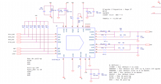
Hello, we have just implemented the DAC81402 converter in our assembly, driven by our STM32G431CBU processor.
Of course, we were inspired by the assembly of your DAC81404 Evaluation Module and BP-DAC81404EVM, BP-DAC61402EVM test boards.
We want to use it in bipolar + or - 10VDC mode. For the moment, we have validated its power supply and started programming (initialization and control), but we are unable to generate output voltages.
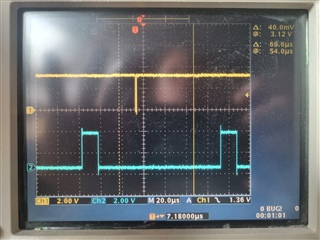
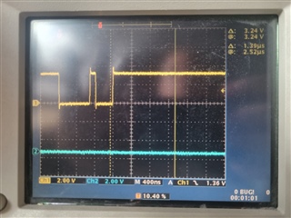
Although we have verified and measured it, could you please confirm our schematic?

Also, here are our lines of code

void DAC81402_Init(void) {

// CLR bas puis haut (reset logiciel)

HAL_GPIO_WritePin(DAC_CLR_GPIO_Port, DAC_CLR_Pin, GPIO_PIN_RESET);

HAL_Delay(1);

HAL_GPIO_WritePin(DAC_CLR_GPIO_Port, DAC_CLR_Pin, GPIO_PIN_SET);

// RST haut (actif à 0 normalement, donc on relâche à 1)

HAL_GPIO_WritePin(DAC_RST_GPIO_Port, DAC_RST_Pin, GPIO_PIN_SET);

HAL_Delay(10);

// GAIN = 0x0000 → tous les DACs en ±10.8 V

DAC81402_WriteRegister(0x04, 0x0000);

// Activer toutes les sorties (0 = activé)

DAC81402_WriteRegister(0x02, 0x0000);

// Optionnel : forcer une impulsion LDAC

HAL_GPIO_WritePin(DAC_LDA_GPIO_Port, DAC_LDA_Pin, GPIO_PIN_RESET);

HAL_Delay(1);

HAL_GPIO_WritePin(DAC_LDA_GPIO_Port, DAC_LDA_Pin, GPIO_PIN_SET);

}

void DAC81402_WriteRegister(uint8_t regAddr, uint16_t value)

{

uint8_t txBuffer[3];

// Trame 24 bits : 8 bits adresse + 16 bits data

txBuffer[0] = regAddr & 0x7F; // MSB: adresse du registre (bit 7 = 0 pour écriture)

txBuffer[1] = (value >> 8) & 0xFF; // Données, MSB

txBuffer[2] = value & 0xFF; // Données, LSB

// Baisser SYNC (actif bas)

HAL_GPIO_WritePin(DAC_SYNC_GPIO_Port, DAC_SYNC_Pin, GPIO_PIN_RESET);

// Transmission SPI

HAL_SPI_Transmit(&hspi1, txBuffer, 3, HAL_MAX_DELAY);

// Remonter SYNC (fin de trame)

HAL_GPIO_WritePin(DAC_SYNC_GPIO_Port, DAC_SYNC_Pin, GPIO_PIN_SET);

}

void DAC81402_SetOutput(uint8_t dac_channel, uint16_t value) {

// dac_channel = 0 → DAC A, 1 → DAC B, etc.

if (dac_channel > 3) return;

uint8_t reg = 0x08 + dac_channel; // 0x08 = DAC A, 0x09 = DAC B, etc.

DAC81402_WriteRegister(reg, value);

}

And We launch in main

// Sortie A → +10V, Sortie B → -10V

DAC81402_SetOutput(0, 0xFFFF); // DAC A → +10V

//DAC81402_SetOutput(0, 61867); // ≈ +10 V

DAC81402_SetOutput(1, 0x0000); // DAC B → -10V

//DAC81402_SetOutput(1, 1700); // ≈ -10 V


Do you have any recommendations to help us move forward?

Thank you for your help.
Have a nice day.

  • ha yes i forget, R76 et R73 are absents

  • Hi Laurent,

    Schematics looks to be okay and the the code doesn't looks proper.

    I would suggest to write one SPI command and verify it  oscilloscope to make sure the patterns are okay.

    You can follow the below write command sequence to get the voltage on the DAC outputs.

    a) Write 0x0A84 in SPICONFIG (0x03) -  to power-up the DAC81402 device 

    b) Write 0x3F00 in GENCONFIG (0x04) - if you are using internal reference, else ignore this

    c) Write 0x0000 in DACPWDN (0x09) - to power-up the individual DAC channels

    d) Write 0xFFFF in DACn_DATA (n = 0x11 or 0x12) -  to configure the DAC A or B channel outputs to 5 V 

    If you are able to get the DAC output, try to configure the the DAC range for +/-10V span.

     
    Thanks,
    Sanjay

  • Hello Sanjay, and thank you for your feedback.

    We are generating SPI frames on the SDIN, SCLK, and SDIN busses, but we are unable to get the converter to work. Initially, we are unable to initialize it.

    We are using the internal reference. We don't have 2.5V in REFIO?

    void DAC81402_Init(void) {

    // CLR bas puis haut (reset logiciel)

    HAL_GPIO_WritePin(DAC_CLR_GPIO_Port, DAC_CLR_Pin, GPIO_PIN_RESET);

    HAL_Delay(1);

    HAL_GPIO_WritePin(DAC_CLR_GPIO_Port, DAC_CLR_Pin, GPIO_PIN_SET);

    // RST haut (actif à 0 normalement, donc on relâche à 1)

    HAL_GPIO_WritePin(DAC_RST_GPIO_Port, DAC_RST_Pin, GPIO_PIN_SET);

    HAL_Delay(10);

    // 3. Activer la référence interne (Register 0x04, Bit 14 = 1)

    DAC81402_WriteRegister(0x04, 0x4000); // REF-DACEN = 1 → active la référence interne

    // 4. Configurer les gains pour ±10V (Register 0x0A)

    // Bits : DACB = 0110, DACA = 0110 → 0x0660

    DAC81402_WriteRegister(0x0A, 0x0660);

    // 5. Activer toutes les sorties DAC (Register 0x09 = 0x0000)

    DAC81402_WriteRegister(0x09, 0x0000);

    // Optionnel : forcer une impulsion LDAC

    HAL_GPIO_WritePin(DAC_LDA_GPIO_Port, DAC_LDA_Pin, GPIO_PIN_RESET);

    HAL_Delay(1);

    HAL_GPIO_WritePin(DAC_LDA_GPIO_Port, DAC_LDA_Pin, GPIO_PIN_SET);

    }

    AVEC 

    void DAC81402_WriteRegister(uint8_t regAddr, uint16_t value)

    {

    uint8_t txBuffer[3];

    // Trame 24 bits : 8 bits adresse + 16 bits data

    txBuffer[0] = regAddr & 0x7F; // MSB: adresse du registre (bit 7 = 0 pour écriture)

    txBuffer[1] = (value >> 8) & 0xFF; // Données, MSB

    txBuffer[2] = value & 0xFF; // Données, LSB

    // SYNC bas pour démarrer la communication

    HAL_GPIO_WritePin(DAC_SINC_GPIO_Port, DAC_SINC_Pin, GPIO_PIN_RESET);

    HAL_SPI_Transmit(&hspi1, txBuffer, 3, HAL_MAX_DELAY);

    HAL_GPIO_WritePin(DAC_SINC_GPIO_Port, DAC_SINC_Pin, GPIO_PIN_SET);

    }


    SDIN at the top and SCLK at the bottom

  • HI Laurent,

    I think you are skipping the step a) Write 0x0A84 in SPICONFIG (0x03) -  to power-up the DAC81402 device. Please check again.

    Also it's very difficult for me to make sense from the scope capture. Please share the scope snapshot of the SPI signals - CSz, SDIN, SCLK and SDO in a single frame for write commands mentioned below.

    a) Write 0x0A84 in SPICONFIG (0x03) -  to power-up the DAC81402 device 

    b) Write 0x3F00 in GENCONFIG (0x04) - if you are using internal reference, else ignore this

    c) Write 0x0000 in DACPWDN (0x09) - to power-up the individual DAC channels

    d) Write 0xFFFF in DACn_DATA (n = 0x11 or 0x12) -  to configure the DAC A or B channel outputs to 5 V


    Thanks,
    Sanjay

  • Hello Sanjay, and thank you for your feedback.
    I'm not well-equipped with an oscilloscope; it's not recent, and I'm missing some waveforms I ordered. I don't have an analyzer, so for now, I'm validating the signals by alternating between viewing the SINC and SDIN signals. Actually, I wasn't configuring SPICONF. I thought it would be valid by default, and I'll look into that...

    Can you confirm the initialization:

    CLR to 0 then
    CLR to 1

    RST to 1

    Write 0x0A84 in SPICONFIG (0x03) - to power up the DAC81402 device. I don't really need to access this register; it's just used to validate the SDO, and the rest is either reserved or used for fault detection, returning to "FAULT." For now, I'm trying to write, so I'm only using SDI, which validates by default unless there's an error.

    Write 0x3F00 in GENCONFIG (0x04) - if you're using internal reference, why 0x3F00? Just set Bit 14 to 0 for the internal reference, 0x0000 in 0x04 to use the internal reference.

    Write 0x0660 IN DACRANGE (0x0A) - For more or less 10Vdc

    Write 0x0000 in DACPWDN (0x09) - To power up the individual DAC channels, okay, I agree.

    Optional
    LDAC to 0
    LDAC to 0

    AND My Commands
    Write 0xFFFF in DACn_DATA (n = 0x11 or 0x12) - To configure the DAC A or B channel outputs to 10V

    Is that good?

    Best regards

    Laurent Ifergane

  • HI Laurent,       

    This looks perfect, please try it out and let me know if you are still facing issue.


    Thanks,
    Sanja