Tool/software:
Dear sir/madam,
I am having trouble getting the DAC5256AEVM bring up. I have shared the status information of my setup below:
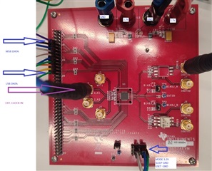
- I set Mode High and Sleep - GSET are connected to Gnd pins
- I generated the data and clock that DAC5256AEVM will use from the FPGA.
- I generated a 10MHz Clock signal from the Clock Capable pin and gave it to the J5 WRT1 SMA input. I provided this connection with pin to sma.
- I connected the sine of the 1MHz sinusoidal signal generated with the 10MHz clock (with FPGA) to the DA pin and the cosine to the DB pin to the data pins. I provided these connections with jumpers.
- I send new data to eval board on the falling edge of the fpga external clock.
- I shared the grounds between the FPGA and the EVM. I also connected the supply voltages correctly.
- We tried it with a balun, but when we couldn't get the result, we removed the balun at IOUTA1/2 and made changes to the hardware so that R2, R28, R7 = 0R , R3 = DNP
- Additionaly I use ZedBoard as FPGA
Despite doing these, I cannot get any output signal at IOUTA/B. Where exactly is my problem?
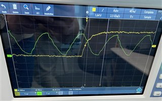 ** green line: fpga external clock, yellow line: data msb input