This thread has been locked.

If you have a related question, please click the "Ask a related question" button in the top right corner. The newly created question will be automatically linked to this question.

DAC80502: the overshoot at DAC output happen when the output setting change from 0V to 2.5V.

Part Number: DAC80502
Other Parts Discussed in Thread: DAC80501

Tool/software:

Hello team,

My customer is using DAC80502 on their prototype.

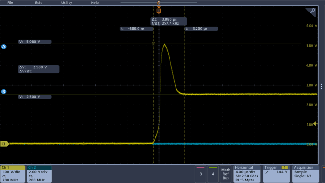
They have some prototype board, but one of some DAC80501 has a problem with overshoot output when the output setting change from 0V to 2.5V as the following picture.
0x090000 (DAC-B : 0V) → 0x098000 (DAC-B :  2.5V) 
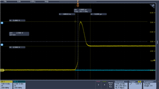
<Zoomed picture>
/resized-image/__size/1037x586/__key/communityserver-discussions-components-files/73/8780.png

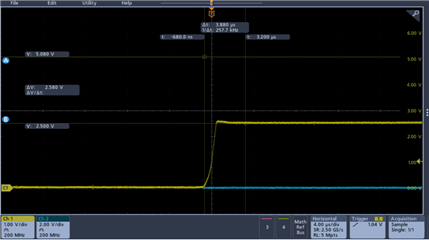
But when they change the DAC output from 0.001V to 2.5V, the overshoot did not happen as the following.
0x09000D (DAC-B : 0.001V) → 0x098000 (DAC-B: 2.5V)

<Zoomed picture>
/resized-image/__size/1044x240/__key/communityserver-discussions-components-files/73/7142.png

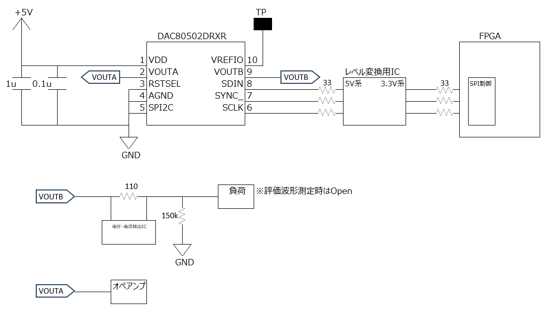
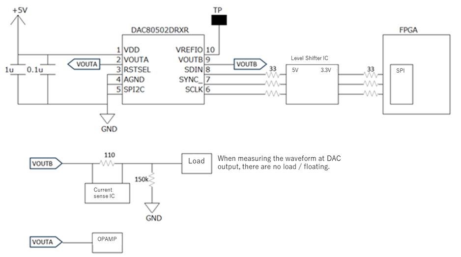
DAC80502 schematics is the following.
/resized-image/__size/1114x623/__key/communityserver-discussions-components-files/73/1856.png

Additional information is the following.
VDD = 5V DC supply
RSTSEL = GND
VREFIO = floating (Because they use Internal Reference)
SPI is used.
This DAC80502 in this prototype always observe  the overshoot , but the overshoot did not happen in others. Is that abnormal or failure about the prototype DAC that is causing overshoot? Is there a way to fix it? 

Your advice is appreciated.

Best Regards,
Akihisa Tamazaki


  • Hello Akihisa-san, 

    Can you share more details about the output load? I see some resistors in the schematic but I'm not sure what the other blocks are. 

    Is there something that changed between the first prototype and this one? Is it possible to do an A-B-A swap between a known bad device/board and a good device/board to see if the issue follows the device or the board? 

    How many units were tested in the prototypes, and how many units are seeing the issue?

    It's possible that the devices seeing the issue have a negative offset and are seeing excess overshoot due to the op amp needing to drive out of the negative rail (ground), but I am a bit surprised by the magnitude of the overshoot..  

    Best,

    Katlynne Jones

  • Katlynne-san,

    Thank you for your reply.

    Can you share more details about the output load? I see some resistors in the schematic but I'm not sure what the other blocks are. 

    The customer observe VOUTB waveform as the following circuit. there are 2 resisters as the load, but there are no load when the customer checked the waveform of VOUTB.
    /resized-image/__size/938x523/__key/communityserver-discussions-components-files/73/65016.png

    The customer mentioned that they have confirmed that the 110 Ω and 150 k Ω loads are operating normally.

    Is there something that changed between the first prototype and this one? Is it possible to do an A-B-A swap between a known bad device/board and a good device/board to see if the issue follows the device or the board? 

    The customer checked 5 boards. Then they found this phenomenon in the only one board.
    They think that  it is highly likely that the reproduction will not be possible if the swap is carried out.
    As mentioned below, even though it goes down to 5V at 0V → 2.5V, it does not happen at 0.001V → 2.5V.
    Therefore, they believe that the possibility of the impact of the VOUTB connection load is low.


    They have one more question. Would you please confirm if there is anything you can think of in the settings for the IC?  If you think that this IC is abnormal one, please let me know.

    Your advice is appreciated.

    Best Regards,
    Akihisa Tamazaki

  • Hello Akihisa-san, 

    It sounds like the device could be damaged then. An A-B-A swap would confirm this and also rule out any potential issues due to bad soldering. If the customer would move forward with a quality return (assuming the device is from an authorized distributor), then we would request them to try the A-B-A swap before shipping us the sample. 

    It is typical for a DAC output to see larger overshoot when driving out of the negative (or positive) rail which could explain why the issue is not seen when driving from slightly above the rail, but the magnitude of the overshoot in the customer's scope plot is much more than expected. 

    There are no register settings that would cause this type of behavior. 

    Best,

    Katlynne Jones

  • Katlynne-san,

    Thank you very much for your comment.
    The customer also think that this device have damaged.

    It is typical for a DAC output to see larger overshoot when driving out of the negative (or positive) rail which could explain why the issue is not seen when driving from slightly above the rail, but the magnitude of the overshoot in the customer's scope plot is much more than expected. 

    The customer seems to not to a little believe your comment. Because when changing from 0.01V to 2.5V, there will be no overshoot, but when changing from 0V to 2.5V, there will be a large overshoot. Customer wants to know if it is better to think that the buffer part of the DAC output has been damaged than the control part of DAC. so would you please advise us if it is a possibility where in the DAC may have damaged. 

    Your help is appreciated.

    Best Regards,
    Akihisa Tamazaki

  • Hello Akihisa-san, 

    What part of my comment is not believed? Overshoot when driving out of the rail is a typical phenomenon in op amps with a negative offset, but like I said the magnitude of the overshoot is much more than expected in this case. I don't really have much insight into which part of the DAC is actually damaged here, but you can submit a quality return, and the quality team can look more into it. 

    Best,

    Katlynne Jones

  • Katlynne-san,

    Thank you for your comment.
    I will discuss with the customer again, then I will ask  you again.

    Best Regards,
    Akihisa Tamazaki