This thread has been locked.

If you have a related question, please click the "Ask a related question" button in the top right corner. The newly created question will be automatically linked to this question.

ADS8361: We found count variation in reading

Part Number: ADS8361

Tool/software:

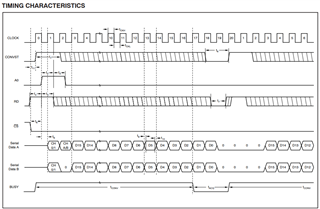
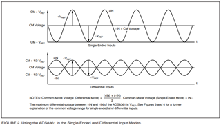
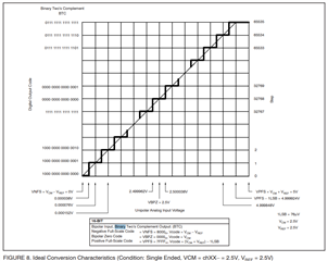
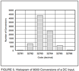
We are observing a count variation in the range of 100–200 LSBs, even when the input channels are shorted. This indicates potential noise, offset, or stability issues within the measurement system. Kindly suggest methods to minimize this variation and enhance measurement accuracy.

  • This is our code please review and suggest if we go any wrong way. Please rectify it for mode II.

    We waiting for your positive feedback.


    //#ifndef _EXAMPLE_FILE_NAME_H /* Guard against multiple inclusion */ //#define _EXAMPLE_FILE_NAME_H /* ************************************************************************** */ /* ************************************************************************** */ /* Section: Included Files */ /* ************************************************************************** */
    /* ************************************************************************** */ /* This section lists the other files that are included in this file. */ /* TODO: Include other files here if needed. */ /* Provide C++ Compatibility */ #ifdef __cplusplus extern "C" { #endif /* ************************************************************************** */ /* ************************************************************************** */ /* Section: Constants */ /* // DEVCFG3 #pragma config FMIIEN = OFF // Ethernet MII Enable #pragma config FETHIO = ON // Ethernet I/O Pin Select #pragma config PGL1WAY = OFF // Permission Group Lock One Way Configuration #pragma config PMDL1WAY = OFF // Peripheral Module Disable Configuration #pragma config IOL1WAY = OFF // Peripheral Pin Select Configuration #pragma config FUSBIDIO = OFF // USB USBID Selection */ // DEVCFG2 #pragma config FPLLIDIV = DIV_1 // System PLL Input Divider #pragma config FPLLRNG = RANGE_8_16_MHZ // System PLL Input Range #pragma config FPLLICLK = PLL_FRC // System PLL Input Clock Selection #pragma config FPLLMULT = MUL_94 // System PLL Multiplier//20 #pragma config FPLLODIV = DIV_4 // System PLL Output Divisor//8 //finally clk is 188mhz #pragma config UPLLFSEL = FREQ_24MHZ // USB PLL Input Frequency Selection //#pragma config UPLLEN = ON // USB PLL Enable // DEVCFG1 #pragma config FNOSC = SPLL // Oscillator Selection Bits #pragma config DMTINTV = WIN_127_128 // DMT Count Window Interval #pragma config FSOSCEN = OFF // Secondary Oscillator Enable #pragma config IESO = OFF // Internal/External Switch Over #pragma config POSCMOD = OFF // Primary Oscillator #pragma config OSCIOFNC = ON // CLKO Output Signal #pragma config FCKSM = CSDCMD // Clock Switching and Monitor Selection #pragma config WDTPS = PS1048576 // Watchdog Timer Postscaler #pragma config WDTSPGM = STOP // Watchdog Timer Stop During Flash Programming #pragma config WINDIS = NORMAL // Watchdog Timer Window Mod #pragma config FWDTEN = OFF // Watchdog Timer Enable #pragma config FWDTWINSZ= WINSZ_25 // Watchdog Timer Window Size #pragma config FDMTEN = OFF // Deadman Timer Enable /* DEVCFG0 */ //#pragma config DEBUG = ON // Background Debugger #pragma config DEBUG = ON // Background Debugger on 11.21.17 #pragma config JTAGEN = OFF // JTAG Port #pragma config ICESEL = ICS_PGx2 // ICE/ICD Communication Channel #pragma config FECCCON = DYNAMIC // ECC ENABLE #pragma config CP = OFF // Code Protect /* #pragma config TRCEN = OFF // Trace feature in CPU #pragma config BOOTISA = MIPS32 // MIPS32 or MICROMIPS #pragma config FECCCON = OFF_UNLOCKED // Dynamic Flash ECC #pragma config FSLEEP = OFF // Flash Sleep Mode #pragma config DBGPER = PG_ALL // Allow CPU access to all permission regions #pragma config EJTAGBEN = NORMAL // Normal EJTAG functionality */ /* // DEVCP0 #pragma config CP = OFF // Code Protect #pragma config_alt FWDTEN=OFF #pragma config_alt USERID = 0x1234u */ /* ************************************************************************** */ /* ************************************************************************** */ /* A brief description of a section can be given directly below the section banner. */ /* ************************************************************************** */ /** Descriptive Constant Name @Summary Brief one-line summary of the constant. @Description Full description, explaining the purpose and usage of the constant. <p> Additional description in consecutive paragraphs separated by HTML paragraph breaks, as necessary. <p> Type "JavaDoc" in the "How Do I?" IDE toolbar for more information on tags. @Remarks Any additional remarks */ //#define EXAMPLE_CONSTANT 0 // ***************************************************************************** // ***************************************************************************** // Section: Data Types // ***************************************************************************** // ***************************************************************************** /* A brief description of a section can be given directly below the section banner. */ // ***************************************************************************** /** Descriptive Data Type Name @Summary Brief one-line summary of the data type. @Description Full description, explaining the purpose and usage of the data type. <p> Additional description in consecutive paragraphs separated by HTML paragraph breaks, as necessary. <p> Type "JavaDoc" in the "How Do I?" IDE toolbar for more information on tags. @Remarks Any additional remarks <p> Describe enumeration elements and structure and union members above each element or member. */ // typedef struct _example_struct_t { // /* Describe structure member. */ // int some_number; // // /* Describe structure member. */ // bool some_flag; // // } example_struct_t; // ***************************************************************************** // ***************************************************************************** // Section: Interface Functions // ***************************************************************************** // ***************************************************************************** /* A brief description of a section can be given directly below the section banner. */ // ***************************************************************************** /** @Function int ExampleFunctionName ( int param1, int param2 ) @Summary Brief one-line description of the function. @Description Full description, explaining the purpose and usage of the function. <p> Additional description in consecutive paragraphs separated by HTML paragraph breaks, as necessary. <p> Type "JavaDoc" in the "How Do I?" IDE toolbar for more information on tags. @Precondition List and describe any required preconditions. If there are no preconditions, enter "None." @Parameters @param param1 Describe the first parameter to the function. @param param2 Describe the second parameter to the function. @Returns List (if feasible) and describe the return values of the function. <ul> <li>1 Indicates an error occurred <li>0 Indicates an error did not occur </ul> @Remarks Describe any special behavior not described above. <p> Any additional remarks. @Example @code if(ExampleFunctionName(1, 2) == 0) { return 3; } */ // int ExampleFunction(int param1, int param2); /* Provide C++ Compatibility */ #ifdef __cplusplus } #endif //#endif /* _EXAMPLE_FILE_NAME_H */ /* ***************************************************************************** End of File */ #include <xc.h> #define ADC_CHIP_SELECT LATDbits.LATD9 #define ADC_CONV_START LATDbits.LATD2 #define ADC_BUSY PORTFbits.RF5 void Port_Init(void); void SPI1_Init(void); void Delay(int); long int SPI_Read(void); void ADC_SAMPLE_Read(void); void Sort(unsigned int ); unsigned int TEMP_1,TEMP_2,CH0A_ADC_DATA,CH0B_ADC_DATA; unsigned short int SAMPLE_R[1000],count; unsigned char iGloble = 0; int main(void) { Port_Init(); SPI1_Init(); Delay(10); while(1) { ADC_CONV_START = 0; //ADC Conversion Start make LOW. Delay(1); ADC_SAMPLE_Read(); ADC_CONV_START = 0; } return 1; } void Port_Init(void) { TRISDbits.TRISD9 = 0; // CS TRISDbits.TRISD2 = 0; // CONV_START TRISFbits.TRISF5 = 1; // BUSY TRISEbits.TRISE6 = 1; // 10 KC pin Check } void SPI1_Init(void) { //SPI1PORT_REMAP(); //Re-mapping the ports for SPI1 : ad7606 RPD11R = 0x00000005; //MOSI => SDO1 as output Controller PIN = 45 (RD11) SDI1R = 0x00000002; //MISO => SDI1 as input Controller PIN = 41 (RF4) TRISDbits.TRISD11 = 0; //Set pin direction as a output. Delay(2); //2 mSec Delay // Device Configured as Master (SPI1 Used) SPI1CON = 0; //Stop & reset SPI1 SPI1STATbits.SPIROV = 0; //Clear overflow flag //initialize SPI registers SPI1CONbits.ON = 1; //SPI ON // SPI1CONSET = 00 << 10; //8 Bit SPI Mode SPI1CONbits.MODE16 = 0; //For 16 bit data make MODE16 = 1 and MODE32 = 0 SPI1CONbits.MODE32 = 1; //For 32 bit data make MODE32 = 1 and MODE16 = 0 SPI1CONbits.SMP = 1; //Data input sample (Input data sampled at end of data output time) SPI1CONbits.CKE = 1; //CLK Edge (output data changes on transition from active clock state to Idle clock state) SPI1CONbits.CKP = 0; //CLK Polarity (IDEL Low Level,Active High Level) SPI1CONbits.MSTEN = 1; //Master PIN Enable //change system clock 188MHZ // Fpb (94 MHz) = (System CLK/2) = (188 MHz / 2) = 94MHz SPI1BRG = 0x16; //SPI CLK = 2MHz @ SYSTEM_CLK 188MHz // SPI1BRG = 0x2E; //SPI CLK = 1MHz @ SYSTEM_CLK 188MHz // SPI1BRG = 0x20; //1468749 mhz SPI1CON2 = 0x00000000; //Not configured Delay(25); } void Delay(int delay) { unsigned int iCount, iDelay; for (iCount = 0; iCount < delay; iCount++) { for (iDelay = 0; iDelay < 100000; iDelay++); } } long int SPI_Read(void) { SPI1BUF = 0x00; //Load buffer with 0 as we only want to receive data //while (SPI1STATbits.SPIBUSY); //Wait until SPI transmission complete while (!SPI1STATbits.SPIRBF); return SPI1BUF; //Return character received } void ADC_SAMPLE_Read(void) { int n,jCounter; for(n = 0; n < 1000; n++) { TEMP_1 = TEMP_2 = 0; TEMP_1 = SPI_Read(); //Read in 32 bit ADC_CONV_START = 1; for(jCounter = 0; jCounter < 100; jCounter++); ADC_CONV_START = 0; TEMP_2 = SPI_Read(); ADC_CONV_START = 1; for(jCounter = 0; jCounter < 100; jCounter++); ADC_CONV_START = 0; Sort(TEMP_1); Sort(TEMP_2); SAMPLE_R[n] = CH0A_ADC_DATA; while (!PORTEbits.RE6); }//end of for loop TEMP_1 = 0; } void Sort(unsigned int data) { unsigned int ADC_DATA; int CH = (data & 0x060000000); //FIND the channel. ADC_DATA = (data >> 13)& 0x0FFFF; //Set the data. switch (CH) { case 0x00000000: //CH0A chaannel value CH0A_ADC_DATA = ADC_DATA; count += 1; break; case 0x20000000: //CH0B channel value CH0B_ADC_DATA = ADC_DATA; count += 1; break; } if (count == 2) { count = 0; } }//end of sort Function
  • Hello Shushant, 

    Welcome to TI's E2E forum! Thank you for posting your question!

    I have some follow-up asks:

    • Could you kindly share a schematic of the ADS8361 in your system?
    • As well as the Mode the device is configured to (M0 and M1 configuration)?
    • Are you supplying an external reference or are is the internal reference being used? 
    • Do you have an oscilloscope shot of what the digital signals look like during the data transfer? 

    From what I can see in the code it seems the data should be decoded back correctly, but I want to confirm about the SPI protocol configuration

    SPI1CONbits.CKE = 1; //CLK Edge (output data changes on transition from active clock state to Idle clock state)

    the data on SDO transitions on the rising edge and is valid on the falling edge.  is setting SPI1CONbits.CKE = 1 configured to read data on the falling edge (active to idle clock stage) or does this make it so it reads back the the opposite transitions ? 

    Best regards, 

    Yolanda

    • Ya sure, I will share the Schematic.
    • We are using Mode 2. i.e. A0= 0, M0= 0, M1=1.
    • We are using Internal Reference.
    • Yes, we can see the pulses on controller pins. (PIC32MZ2048EFH064)
  • R_DATA_2_120000.xlsx

    Data count we fetched with variation and graph plotted for the same.

  • In all settings we are not checking Busy pin. we fetched the data on synchronized with RD pin .

  • Thank you for sharing Shshant!

    I think the code looks fine, synchronizing to the RD pin should work. 

    Looking at you schematic, could you confirm what output signal from the DIff Amps looks like?  It seems like the ADS8361 is currently configured in a pseudo differential mode. Using it like this should be fine, but it does require that the signal at the AIN+ still maintain a common mode of VREF as well.  Being that the supplies for the Diff-Amps are +/-5V and the REF pin of those Diff Amps is tied to GND,  I wanted to make sure they were still being offset to stay within the common mode range?

    With the internal reference so long as the LK1 & LK18 are shorted it should be fine too. 

    Best regards, 

    Yolanda

  • Hello Shshan, 

    Another note for the code actually, the data format is in 2s compliment, has this been accounted for in your code? 

    I was looking through the data file shared and it seems like they are all negative numbers ,so just wanted to confirm. 

    Is the input at the ADC negative or lower than the VREF? 


    Best regards, 

    Yolanda

  • Thank you  for your reply.

    We are using single ended mode (A0 & B0 with AOut Only). and AIN- terminations tied to reference pin and reference link also shorten so we get 2.5V reference. That's why we get the count above 32767. 

    We taken 60000 samples with 10 KHz and SPI Speed is 2 MHz.

    What is your experience about count variation?? What is the tolerance band for data conversion?

    Please share if you have any sample PCB board routing on which we will get count without variation?? Or you observed same type of variation??

    I share you the PCB routing image if you have any suggestion please give us your inputs.

  • Hello Shshan, 

    We taken 60000 samples with 10 KHz and SPI Speed is 2 MHz.

    what is the amplitude of this signal? does it also have a common mode of 2.5V? Could you share how this looks like on an oscilloscope 

    What is your experience about count variation?? What is the tolerance band for data conversion?

    With a DC input there is a code spread of a about ±2.5 codes/lsbs. 

    .

    Could you please help point where the ADC is here as well as any components surrounding the ADC? If a schematic is available that would be helpful too.

    Does the input have an RC filter? What is the driving circuit for the ADC input? 

    The layout can be straight forward, there is no high speed concern for this device. The layout for the  ADS8361EVM  (U1 is the ADS8361)

    Best regards, 

    Yolanda