Part Number: DAC3484
Other Parts Discussed in Thread: CDCE62005, , DAC3482
Tool/software:
Hello
I am configuring a system consisting a FPGA board (Avnet Microzed 7020), connected to a custom board consisting 2 DAC3484 and a CDCE62005.
My initial goal is to understand the utilization of a single DAC, and I am trying to receive an output (measured by my scope) of a 5MHz sine wave given by my NCO (+the phase of the DDS).
the FPGA board is configured to output a 16-bit data signal in sign-and-magnitude representation, where rising edge shows the sine wave phase, and falling edge shows the cosine wave phase as the output.
my CDCE62005 configuration (connected to a primary clock of 100MHz):
0xEB40032, // Register 0- DACCLK1 400MHz
0xEB84030, // Register 1- DACCLK2 100MHz (currently irrelevant because I am concentrating on DAC1)
0xEB84030, // Register 2- Irrelevant
0xEB3C030, // Register 3- -OSTR 6.25 MHz
0xEB84031, // Register 4- FPGACLK 100 MHz
0x10080BF, // Register 5
0x04BE008, // Register 6
0xBD0037F // Register 7
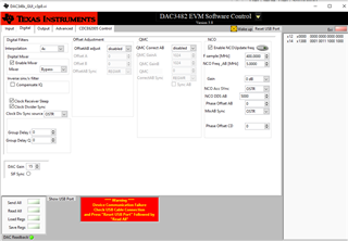
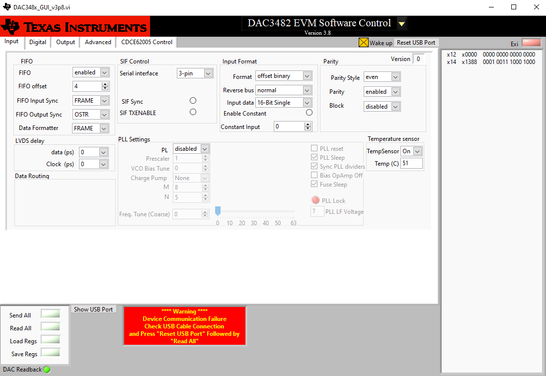
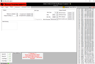
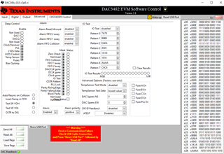
DAC configuration:
Reading the datasheet, I got these equations: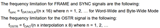
hence the F_OSTR=F_FRAME=6.25MHz = F_DACCLK/64
because the input to the DAC uses only two channels, I enabled Dual mode and measured the B-channel with my scope.
I disabled the PLL (config24/bit10->0), chose OSTR as sync source in the config31 control (0x2220), and enabled mixer and NCO (config2:0xF050).
additional information about my system:
* F_DATACLK= 100MHz
*Interpolation is 4
* NCO phase word is 0x03333333
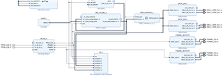
* my relevant part of my FPGA system looks like this:
* My DAC configuration:
x00 x029F 0000 0010 1001 1111
x01 x050E 0000 0101 0000 1110
x02 xF070 1111 0000 0111 0000
x03 xF001 1111 0000 0000 0001
x04 x0000 0000 0000 0000 0000
x05 x0000 0000 0000 0000 0000
x06 x3300 0011 0011 0000 0000
x07 xFFFF 1111 1111 1111 1111
x08 x0000 0000 0000 0000 0000
x09 x8000 1000 0000 0000 0000
x0A x0000 0000 0000 0000 0000
x0B x0000 0000 0000 0000 0000
x0C x0400 0000 0100 0000 0000
x0D x0400 0000 0100 0000 0000
x0E x0400 0000 0100 0000 0000
x0F x0400 0000 0100 0000 0000
x10 x0000 0000 0000 0000 0000
x11 x0000 0000 0000 0000 0000
x12 x0000 0000 0000 0000 0000
x13 x0000 0000 0000 0000 0000
x14 x3333 0011 0011 0011 0011
x15 x0333 0000 0011 0011 0011
x16 x6666 0110 0110 0110 0110
x17 x2666 0010 0110 0110 0110
x18 x280F 0010 1000 0000 1111
x19 x0840 0000 1000 0100 0000
x1A x0030 0000 0000 0011 0000
x1B x0800 0000 1000 0000 0000
x1C x0000 0000 0000 0000 0000
x1D x0000 0000 0000 0000 0000
x1E x1111 0001 0001 0001 0001
x1F x1110 0001 0001 0001 0000
x20 x2401 0010 0100 0000 0001
x22 x1B1F 0001 1011 0001 1111
x23 x07FF 0000 0111 1111 1111
x24 x0000 0000 0000 0000 0000
x25 x7A78 0111 1010 0111 1000
x26 xB6B6 1011 0110 1011 0110
x27 xEAEA 1110 1010 1110 1010
x28 x4545 0100 0101 0100 0101
x29 x1A1A 0001 1010 0001 1010
x2A x1616 0001 0110 0001 0110
x2B xAAAA 1010 1010 1010 1010
x2C xC6C6 1100 0110 1100 0110
x2D x0004 0000 0000 0000 0100
x2E x0000 0000 0000 0000 0000
x2F x0000 0000 0000 0000 0000
x30 x0000 0000 0000 0000 0000
x7F x0000 0000 0000 0000 0000
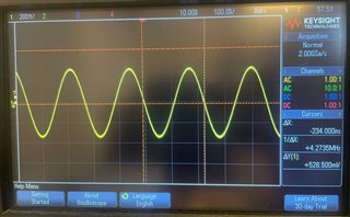
*After setting and resetting the cdce, I get a steady sine wave of 4.27MHz, regardless of the DDS output from the FPGA. for some reason I can not add more pictures to my post so I can not show it.
Some questions:
1. How critical is it to preform a pattern checking upon start?
2. For some reason, setting the 'twos' bit in config2 kills all output, why is that?
3. What could go wrong with my configuration of the DAC.
Thank you in advance,
Tom