This thread has been locked.

If you have a related question, please click the "Ask a related question" button in the top right corner. The newly created question will be automatically linked to this question.

ADS8361: data acquisition time

Part Number: ADS8361

Tool/software:

In a 15-year-old design, we discovered that the analog buffer for data acquisition was too slow. Now we want to extend the data acquisition time in a simple way.

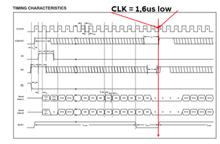
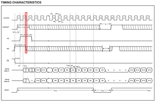
Timing:  Clk Periode: 125ns
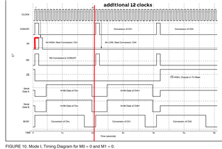
M0, M1 = low


For data acquisition, we want to increase the time from 400 ns to 2 us.

1) Can we create 16 additional CLKs before the next conversion start?

2) Can we insert a low pause of 2 us at CLK19 and then continue with the conversion start.

  • We've now adjusted the timing accordingly.

    Change: 12 additional clocks

    Could this change pose a problem?

     Furthermore, in the datasheet, A0 is always set after Conversion Start.

     We set A0 at the same time as RD and Conversion Start.

     In the datasheet, t2 (address setup time) is only specified as the minimum time.

     Is operating A0 a problem?

  • Hello Guenther, 

    Welcome to TI's E2E Forum! Thank you for posting! 

    I'll answer the main thread questions 1st: 

    1) Can we create 16 additional CLKs before the next conversion start?

    Yes, this should be fine, so long as only the 1st 20 clocks are considered valid for the data (following Table III in datasheet).

    2) Can we insert a low pause of 2 us at CLK19 and then continue with the conversion start.

    Yes as well, will keep the ADC in acquisition time like you intend. 

    Change: 12 additional clocks

    Was it a choice between either adding 12 clocks or inserting the low pause? Either/both should work regardless. 

     We set A0 at the same time as RD and Conversion Start.

    Not a problem at all, as long as it configured at least 15ns before the falling edge of clock 1 (2nd falling edge from CONVST rising edge) and stays in that state 15ns after it will work.

    the status of A0 is latched right at the falling edge of the 1st clock cycle, and to ensure a correct value is latch there is a ±15ns range to ensure proper setting and latching.  The time for t2 & t3 are specified as minimum only because beyond they can theoretically be any value. 

    Best regards, 

    Yolanda

  • Thanks, works fine