This thread has been locked.

If you have a related question, please click the "Ask a related question" button in the top right corner. The newly created question will be automatically linked to this question.

ADS8691: Implementation of the converter for data acquisition

Part Number: ADS8691

Tool/software:

Hello, I'm writing to you to ask if anyone could help me with a problem I'm experiencing and I'm stuck. I'm driving the ADS8691 with my STM32G431CBU MCU via SPI. I'm using it with a bipolar + and - 10Vdc connection, with an internal reference, so it's configured as such, or so I think?!...
So I initialize these registers as such : 
void ADS8691_Init(uint8_t adc_num)
{
     // 1. Plage d’entrée : Bipolaire ±10.24V 0x0001 dans le registre 0x14
     ADS8691_WriteRegister(adc_num, REG_INPUT_RANGE, RANGE_BIPOLAR_10V24);

     // 2. Référence interne activée en permanence 0x0003 dans le registre 0x3C
     ADS8691_WriteRegister(adc_num, REG_REF_CTRL, REF_INTERNAL_ALWAYS_ON);

    // 3. Configuration ligne SDI : mode normal 0x000 dans le registre 0x3E
    ADS8691_WriteRegister(adc_num, REG_SDI_CTRL, SDI_DEFAULT);

     // 4. Configuration ligne SDO : toujours activée 0x000 dans le registre 0x3F
     ADS8691_WriteRegister(adc_num, REG_SDO_CTRL, SDO_DEFAULT);
}


void ADS8691_WriteRegister(uint8_t adc_num, uint8_t reg, uint16_t value)
{
    uint32_t cmd = CMD_WRITE_REGISTER | ((reg & 0x3F) << 16) | (value & 0xFFFF);
    uint8_t tx[4] = {
        (cmd >> 24) & 0xFF,
        (cmd >> 16) & 0xFF,
        (cmd >> 8)  & 0xFF,
        (cmd >> 0)  & 0xFF
    };

    GPIO_TypeDef* sync_port = (adc_num == 1) ? ADC1_SYNC_GPIO_Port : ADC2_SYNC_GPIO_Port;
    uint16_t sync_pin        = (adc_num == 1) ? ADC1_SYNC_Pin        : ADC2_SYNC_Pin;

    sync_port->BSRR = (uint32_t)sync_pin << 16; // SYNC LOW
    HAL_SPI_Transmit(&hspi2, tx, 4, HAL_MAX_DELAY);
    sync_port->BSRR = sync_pin;                 // SYNC HIGH

    HAL_Delay(1);
}
Currently, my converted values ​​aren't changing correctly,
So I tried to verify the initial register writing, but I can't read the data.
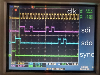
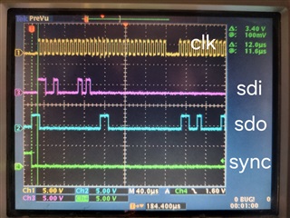
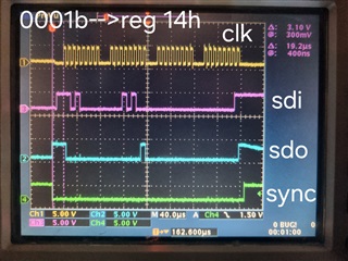
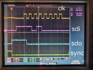
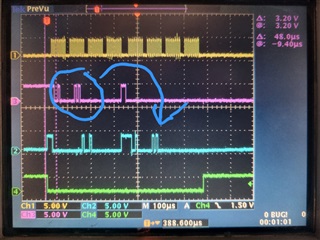
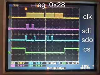
I tried to oscillate the commands from clk, sdi, sdo, and sync, which seem correct to me, but where I should have the register data on the last two bytes of the 32-bit frame, I get nothing.
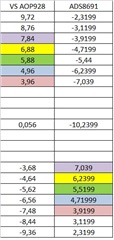
Obviously, I checked the register dedicated to the voltage range 0x14, as well as the ID at 0x00, but others... so I can't get the data... so I don't know if they are configured correctly.
I can see that the ADS8691 is reacting, since it responds in SDO with the same data relating to the register queried in SDI?...
float ADS8691_ReadVoltageFast(uint8_t adc_num, float offset_correction)
{
    GPIO_TypeDef* sync_port;
    uint16_t sync_pin;

    if (adc_num == 1) {
        sync_port = ADC1_SYNC_GPIO_Port;
        sync_pin = ADC1_SYNC_Pin;
    } else {
        sync_port = ADC2_SYNC_GPIO_Port;
        sync_pin = ADC2_SYNC_Pin;
    }

    uint8_t tx_buf[4] = {0x00, 0x00, 0x00, 0x00};  // NOP
    uint8_t rx_buf[4] = {0};

    // SYNC LOW
    sync_port->BSRR = (uint32_t)sync_pin << 16;

    HAL_SPI_TransmitReceive(&hspi2, tx_buf, rx_buf, 4, HAL_MAX_DELAY);

    // SYNC HIGH
    sync_port->BSRR = sync_pin;

    uint32_t raw = ((uint32_t)rx_buf[0] << 24) |
                   ((uint32_t)rx_buf[1] << 16) |
                   ((uint32_t)rx_buf[2] << 8)  |
                   ((uint32_t)rx_buf[3]);

    // Sign-extended 18-bit value extraction
    int32_t code = ((int32_t)(raw << 2)) >> 14;

    float voltage = code * 0.000078125f;

    return voltage + offset_correction;
}
Thank you for your help
Best regards
Laurent Ifergane
  • Hi Laurent,

    Can you get a clearer screen shot of SDI versus SDO?  Maybe zoom in a bit on the 0x28 screen shot to get a clearer idea of how the SPI interface is setup?

  • Hello Tom, and thank you for your invaluable help, because I'm having a hard time here...
    I'm attaching a zoomed-in image where you can see that in SDO, the register addressed in SDI is repeated but doesn't return its value to me?... and so I can't confirm the correct configuration initiated initially, especially when I query the desired bipolar voltage range of +/-10Vdc by putting 0x0001 in reg 0x14 as well as the internal reference.

    A priori, it seems to take the address register into account since it references in SDO, but the data is always at 00... is this because it's really at 00 or not?...

    Ha yes, i forget my function of read register 

    uint16_t ADS8691_ReadRegister(uint8_t adc_num, uint16_t reg_addr)
    {
        GPIO_TypeDef* sync_port;
        uint16_t sync_pin;
    
        if (adc_num == 1) {
            sync_port = ADC1_SYNC_GPIO_Port;
            sync_pin = ADC1_SYNC_Pin;
        } else {
            sync_port = ADC2_SYNC_GPIO_Port;
            sync_pin = ADC2_SYNC_Pin;
        }
    
        uint8_t cmd_byte = 0xC8 | ((reg_addr >> 7) & 0x03);
        uint8_t addr_byte = reg_addr & 0xFF;
    
        uint8_t tx_buf[4] = { cmd_byte, addr_byte, 0x00, 0x00 };
        uint8_t rx_buf[4] = {0};
    
        // SYNC LOW
        sync_port->BSRR = (uint32_t)sync_pin << 16;
    
        // 1) Envoi commande lecture
        HAL_SPI_Transmit(&hspi2, tx_buf, 4, HAL_MAX_DELAY);
    
        // 2) Envoi 4 octets dummy + lecture donnée
        uint8_t dummy[4] = {0,0,0,0};
        HAL_SPI_TransmitReceive(&hspi2, dummy, rx_buf, 4, HAL_MAX_DELAY);
    
        // SYNC HIGH
        sync_port->BSRR = sync_pin;
    
        // Retourne les 2 derniers octets (valeur du registre)
        return ((uint16_t)rx_buf[2] << 8) | rx_buf[3];
    }

  • Hi Laurent,

    I was hoping you could zoom in on the time base with the o'scope - maybe just the first 16 clocks or so?

  • Sorry, I took another measurement.

  • Better!

    If you look closely, you should notice the the phase relationship for SDI and SDO are not aligned.  SDO is valid on the rising SCLK (CPHA=0) while SDI is valid on the falling clock edge (CPHA=1).  Please try changing your controller to use CPOL=0, CPHA=0 and see if that resolves your issues.

  • Hello Tom, thanks for your quick response.

    So I've set my CPOL and CPHA alignment to 0, and I've also reviewed the register read and write commands in detail.

    If I understand correctly, to write, insert the command in MSB:
    D0h, D2h, D4h
    To read:
    C8h or 48h

    So I've corrected my write and read functions.

    Also, in my init function, in addition to the register for the +/-10Vdc voltage range 0001b in 14h, I recall the SDI and SDO registers so as to put:
    0x0 in the 08h register
    0x0 in the 0Ch register

    So I send:
    0xD0140001 for the voltage
    0xD0080000 for SDI
    0xD00C0000 for SDO
    If this is taken into account correctly?...

    Data whose sending is confirmed by observation on the oscilloscope.

    However, when reading my registers, and in particular the choice of my 14h voltage range, I still can't see its contents?...
    In SDO, I can see the repetition of the register querying my steps for the data?...

    Is it necessary to know if I'm writing correctly or reading correctly?...

    i write my register 14h


    And i read 

    But i don't see the data 0001 after ? on the last 16bits

    In fact, unless I'm mistaken, it's as if I were requesting the return of the register with the 48h command in MSB, when I'm actually sending C8h to get only the data.

    uint16_t ADS8691_ReadRegister(uint8_t adc_num, uint16_t reg_addr)
    {
        GPIO_TypeDef* sync_port;
        uint16_t sync_pin;
    
        if (adc_num == 1) {
            sync_port = ADC1_SYNC_GPIO_Port;
            sync_pin = ADC1_SYNC_Pin;
        } else {
            sync_port = ADC2_SYNC_GPIO_Port;
            sync_pin = ADC2_SYNC_Pin;
        }
    
        uint8_t cmd_byte = 0xC8 | ((reg_addr >> 7) & 0x03);
        uint8_t addr_byte = reg_addr & 0xFF;
    
        uint8_t tx_buf[4] = { cmd_byte, addr_byte, 0x00, 0x00 };
        uint8_t rx_buf[4] = {0};
    
        // SYNC LOW
        sync_port->BSRR = (uint32_t)sync_pin << 16;
    
        // 1) Envoi commande lecture
        HAL_SPI_Transmit(&hspi2, tx_buf, 4, HAL_MAX_DELAY);
    
        // 2) Envoi 4 octets dummy + lecture donnée
        uint8_t dummy[4] = {0,0,0,0};
        HAL_SPI_TransmitReceive(&hspi2, dummy, rx_buf, 4, HAL_MAX_DELAY);
    
        // SYNC HIGH
        sync_port->BSRR = sync_pin;
    
        // Retourne les 2 derniers octets (valeur du registre)
        return ((uint16_t)rx_buf[2] << 8) | rx_buf[3];
    }

    best regards

    Laurent Ifergane

  • Hi Laurent,

    Please review the last paragraph on page 41 of the datasheet.  Can you insert a CONVST/CS high between the first and second 32-bit transfer?

  • Oh, okay, I'll test this...

    However, although I haven't yet managed to read my registers, I took a look at my voltage values ​​converted by the ADC in debug mode, and when I checked it, I got 19.7...Vdc for about 9.5...Vdc on its analog input. Without any logic or reasoning, I instinctively subtracted the result of my read function from my conversions by 10, so I went from about 19.7 to 9.7Vdc. Checking other input voltage values, it turns out that the values ​​correspond from +10V to -10V?...
    For now, I can't explain it?.... but I'll dig into this anyway....

    float ADS8691_ReadVoltageFast(uint8_t adc_num, float offset_correction)
    {
        GPIO_TypeDef* sync_port;
        uint16_t sync_pin;
    
        if (adc_num == 1) {
            sync_port = ADC1_SYNC_GPIO_Port;
            sync_pin = ADC1_SYNC_Pin;
        } else {
            sync_port = ADC2_SYNC_GPIO_Port;
            sync_pin = ADC2_SYNC_Pin;
        }
    
        uint8_t tx_buf[4] = {0x00, 0x00, 0x00, 0x00};  // NOP
        uint8_t rx_buf[4] = {0};
    
        // SYNC LOW
        sync_port->BSRR = (uint32_t)sync_pin << 16;
    
        HAL_SPI_TransmitReceive(&hspi2, tx_buf, rx_buf, 4, HAL_MAX_DELAY);
    
        // SYNC HIGH
        sync_port->BSRR = sync_pin;


        //uint32_t raw = ((uint32_t)rx_buf[0] << 24) |
        //               ((uint32_t)rx_buf[1] << 16) |
        //               ((uint32_t)rx_buf[2] << 8)  |
        //               ((uint32_t)rx_buf[3]);
        uint32_t raw = ((uint32_t)rx_buf[0] << 24) | ((uint32_t)rx_buf[1] << 16) |
                       ((uint32_t)rx_buf[2] << 8) | ((uint32_t)rx_buf[3]);
    
    
        code_brut32 = raw ; // test code brut sur 32bit
    
        // Sign-extended 18-bit value extraction
        //int32_t code = ((int32_t)(raw << 2)) >> 14;
    
        int32_t code = (int32_t)(raw >> 14);  // ou (raw >> 14) & 0x3FFFF pour 18 bits signés


        code_brut18 = code ; //test code brut sur 18bit
    
       // float voltage = code * 0.000078125f;
        float voltage = (code * 0.000078125f)-10;
    
        return voltage + offset_correction;
    }

    n the meantime, I corrected the read and write command values ​​on the relevant registers.

    #define CMD_WRITE4_REGISTER       0xD4000000  // Seulement LSB de 16 bits de données sont écrit
    #define CMD_WRITE0_REGISTER       0xD0000000  //
    #define CMD_WRITE2_REGISTER       0xD2000000  // Seulement les 2 octets de poids fort (MSB) des données de 16 bits
    
    #define CMD_READ4_REGISTER       0x48000000   //read
    #define CMD_READC_REGISTER       0xC8000000   //read_hword
    
    // le registre configure la game de tension et ref interne
    #define REG_INPUT_RANGE  0x14
    #define RANGE_BIPOLAR_10V24     0x1
    
    #define REG_SDI_CTRL             0x08   
    #define SDI_DEFAULT              0x0  // SDI active normal
    
    #define REG_SDO_CTRL             0x0C
    #define SDO_DEFAULT              0x0  // SDO enabled always

  • ok, let me know what you find.