Other Parts Discussed in Thread: THS4541, TPS6521905
Tool/software:
We are baffled and frustrated by this. The ADC3910D125 returns data with an apparent noisy high frequency signal with an amplitude of about 15% of the A/D full scale values, when it should be showing a flat line with some noise. Here are the details:
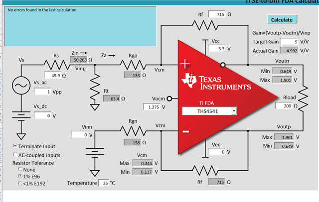
- DC coupled differential signals from THS4541 differential amps connected just like the ADC3910D125 evaluation board except that the output is a simple single pole filter (two 27 ohm resistors and a 22 pF cap across the differential pair at the ADC pins), and we have a higher 4.75X gain on the amp.
- 100 MHz sample clock from our Xilinx FPGA, DC coupled (our layout guy messed up and put the terminating resistor by the ADC rather than the FPGA, but the signal looks stable)
- External REF35120 voltage reference with 10uF and 0.1uF on the Vref pin to the ADC, and 1uF on the NR pin
- 10, 1 and 0.1uF caps on the IOVDD pin 1.8V supply, from a separate LDO than the 1.8V AVDD
- Two 0.1uF caps for the AVDD power pins
We've verified that the digital interface to the FPGA works well with the ramp and inverting ADC data patterns. And the two channels on the DDR bus are properly demultiplexed in the FPGA. And we used a logic analyzer to verify that the data we see is actually on the bus from the ADC.
The mysterious signal we see is always the same amplitude (about 160 counts in 10-bit mode) centered roughly where we would expect it. We can apply an input offset with a DAC driving one leg of the differential input of the THS4541 (the other side of the pair is a single ended scope input which is grounded for these tests) and that shifts the signal up and down as expected. Except that we would expect to see a relatively flat line with a little noise, not an amplitude of 160 counts!.
And get this: even when we short across the differential pair with a solder blob over the cap right next to the ADC pins, the mystery signal is still the same. No change in amplitude.
One board appears to have a noisy 2-3 MHz signal when sampled at 100 MHz, but we believe that is probably an aliased signal, because when we try other sample clocks from the FPGA (110, 90, 80, 70...) we see higher frequencies, but what looks like a single main rough sine wave overlayed with a lot of noise. On another board at 100 Msps, the signal looks more like 6 MHz, but it is also the same amplitude.
We've looked at the Vref, AVDD and IOVDD lines (with 200 MHz scopes, so we might be missing something) and see some noise, but nothing big enough or regular enough to explain the huge signal we see in the data.
Our configuration settings are quite simple. We reset the ADC and then set the registers to use the external voltage reference, and to switch to offset binary rather than 2's complement format on the output data bus. That's it!. The signal is still evident in 2's complement mode, but just formatted differently. And setting to use the internal voltage reference doesn't change anything (though the external reference is still connected to pin 17).
I've attached Excel graphs of the data we see. And as I said, we see the same amplitude and shape to the data even when we short the differential inputs. So it would see to be generated inside the ADC somehow.


Please help! We cannot explain why the ADC seems to be generating this signal in the data that we do not see on the inputs.