This thread has been locked.

If you have a related question, please click the "Ask a related question" button in the top right corner. The newly created question will be automatically linked to this question.

ADC12DJ3200: Multi ADC Synchronization

Part Number: ADC12DJ3200
Other Parts Discussed in Thread: LMX2594

Tool/software:

Hi,

I am trying to phase synchronize the outputs of two ADC12DJ3200 IC's.
I configured the ADC12DJ3200 to JMODE-6 (8-bit, 4-lanes, dual channel) by setting the following parameters-

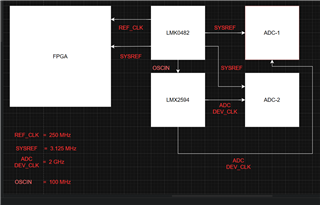
Sampling Frequency = 2 GHz
ADC dev_clk = 2 GHz
line rate = 10 Gsps
JESD ref_clk = 250 MHz
SYSREF Frequency = 3.125 MHz

I have set K = 32 and RBD = 28. I am generating the JESD_ref_clk and sysref from LMK0482 and the ADC clocks from LMX2594. The clocks to both the ADCs are fed from LMX2594 and the sysref
to both the ADCs is fed from LMK0482. The clocks are monitored in the scope for different power cycles and observed to be synchronized.

The ADCs are fed with 900 MHz input signal. When the ADC outputs are plotted, it is observed that the channel outputs within the ADC are synchronized and the outputs between the ADCs are not synchronized.

I tried the SYSREF POSITION DETECTION method for synchronization. The sysref position capture values of two ADCs are different and the values of one of the ADCs is varying from run to run.

ADC-1 -----> The sysref position capture values are
                     0x02C = 1D, 0x02D = 07, 0x02E = 9C

ADC-2 -----> The sysref position capture values are varyng for this ADC.
                      Most commonly observed values are
                      0x02C = F1, 0x02D = FE, 0x02E = D9 and
                      0x02C = F1, 0x02D = FB, 0x02E = FB

It can be observed that the second bit is always zero for the above cases. So, I configured SYSREF_SEL register to 1 (as second bit corresponds to 1 in [7:0]). I plotted the ADC samples again
and observed the same as before. The outputs from ADCs are not phase synchronized though channel outputs within the ADC are synchronized.

I also tried the AUTOMATIC SYSREF CALIBRATION method. I have made the SYSREF_SEL reg to '0', configured the SRC_CFG register and then enabled the SRC_EN. I can observe the SRC_DONE = 1.
But still the outputs from the ADCs are not phase synchronized.

Is there anything to be done so that I can get the phase synchronized outputs from the ADCs?
Kindly request you to resolve this issue.

The ADC configuration register file is attached for reference.

	ADDRESS      DATA

	0x0000 	     0x30
	0x0002 	     0x00
	0x0003 	     0x03
	0x0004 	     0x20
	0x0005 	     0x00
	0x0006 	     0x05
	0x000C 	     0x51
	0x000D 	     0x04			 
	0x0010 	     0x00
	0x0029 	     0x11
	0x0029 	     0x11
	0x002A 	     0x00
	0x002C 	     0x00
	0x002D 	     0x00
	0x002E 	     0x00
	0x0030 	     0xA0
	0x0031 	     0x00
	0x0032 	     0xA0
	0x0033 	     0x00
	0x0038 	     0x00
	0x003B 	     0x00
	0x0060 	     0x00
	0x0200 	     0x00
	0x0061 	     0x00
	0x0201 	     0x06
	0x0202 	     0x1F
	0x0203 	     0x01
	0x0204 	     0x02
	0x0205 	     0x00
	0x0213 	     0x07
	0x0048 	     0x0F
	0x0206 	     0x00
	0x0207 	     0x00
	0x0208 	     0x00
	0x0209 	     0x00
    0x0062 	     0x01
	0x0061 	     0x01
	0x006A 	     0x00
	0x0200 	     0x01
	0x006C 	     0x00
	0x006C 	     0x01		 
	0x0297 	     0x00		 
	0x02C0 	     0x00
	0x02C1 	     0x1F
	0x02C2 	     0x00	

	ADDRESS     DATA
	
	0x0000  	0x30	   
	0x0002  	0x00
	0x0003  	0x03
	0x0004  	0x20
	0x0005  	0x00
	0x0006  	0x05
	0x000C  	0x51
	0x000D  	0x04
	0x0010  	0x00
	0x0029  	0x00
	0x002A  	0x00
	0x0030  	0xA0
	0x0031  	0x00
	0x0032  	0xA0
	0x0033  	0x00
	0x0038 	    0x00
	0x003B  	0x00
	0x0060  	0x00
	0x0200  	0x00
	0x0061  	0x00
	0x0201  	0x06
	0x0202  	0x13
	0x0203  	0x01
	0x0204  	0x02
	0x0205  	0x00
	0x0213  	0x07
	0x0048  	0x0F
	0x0206  	0x00
	0x0207  	0x00
	0x0208  	0x00
	0x0209  	0x00
    0x0062  	0x01
	0x0061  	0x01	   
	0x006A  	0x00
	0x0200  	0x01
	0x006C  	0x00
	0x006C  	0x01
	0x0297  	0x00
	0x02B0  	0x00
	0x02B1  	0x05
	0x02B0  	0x01
	0x02B2  	0x00
	0x02B3  	0x00
	0x02B4  	0x00
	0x02C0  	0x00
	0x02C1  	0x1F
	0x02C2  	0x00

  • Hi Anirudh,

    Please send over a block diagram of your two ADC setup.

    This will be more clear to us on what you are implementing.

    Regards,

    Rob

  • Hi Rob,

    The attached image is the block diagram of my setup.

    Regards,

    Anirudh

  • Thank you Anirudh,

    Are both the sysref and clock lines length matched respectively?

    Regards,

    Rob

  • Yeah Rob,

    Both the sysref and clock lines are length matched and the clocks are also synchronized from power cycle to power cycle.

    Regards, 

    Anirudh

  • Hi Anirudh,

    In re-reading your post closer, I believe you are referring to the signal phase captured or analog phase.

    Keep in mind the sysref will not synchronize the analog phase. All sysref does is synchronize the digital outputs.

    If you want to do a fine analog sync then you can use the devices TAD adjust features and correct for this analog phase offset.

    If you are see differing phase across channels over power cycles then the link is not correctly configured for deterministic latency.

    If this is the case, then please check reg 208, the JESD status register on the ADC this will let you know if sysref is getting captured correctly.

    If this all looks good then it could be an FPGA issue.

    Regards,

    Rob

    PS - I assume your block diagram refers to your board design. Where everything is on one board? Or is this implementation being done with two of our EVMs and an FPGA dev kit?

  • Hi Rob,

    I am checking the phase difference between the digital output samples of the two ADCs. The value in the JESD status register (0x208) is 0x64, which indicates that the JESD link is up.

    Yes Rob, the block diagram refers to my board design and everything is on one board.

    Is there anything else that need to be done for the phase synchronization between the ADCs?

    Regards,

    Anirudh 

  • Hi Anirudh,

    If you are tryin to phase synch the two analog input signals, then we need to look at the frontend, cables, etc.

    Please provide details on this setup. See below...

    Regards,

    Rob

  • Hi Rob,

    I am giving input to the ADC through a 1:4 power divider. The analog outputs from the power divider are monitored in the scope and observed to be in sync. Also the inputs to the ADC are fed from the length matched cables. I have attached the block diagram depicting my setup for the reference.

    Can you confirm whether the ADC registers that I have been writing are correct and are there any registers that have to be written to attain synchronization?

    Regards,

    Anirudh

  • HI Anirudh,

    Unfortunately, the 1:4 power splitter and length matched cables are not enough.

    Need to have phase matched cables, length matched does not equal phase matched.

    Also, you probably want to measure the phase mismatch from the 1:4 splitter using a VNA. 

    One or both is the source of the mismatch error.

    Regards,

    Rob

  • Hi Rob,

    I rearranged the ADC configuration registers and the above issue of varying phase differences is resolved.

    Now I am getting a constant phase difference between the ADC channels from power cycle to power cycle. Can you suggest me a solution such that the phase difference between the channels will be zero?

    Note: The input cables to ADC are length matched and phase matched. The sysref and clocks are also length matched

    Regards,

    Anirudh

  • Hi Anirudh,

    Deterministic latency will guarantee that the phase difference channel to channel is consistent over power cycles. It will not guarantee that the phase offset will be zero, to achieve this you would have to adjust the sampling clock phase to each ADC to get a perfect alignment.

    On the 3200 device there is the TAD feature that can be used to do this.

    Regards,

    Rob