This thread has been locked.

If you have a related question, please click the "Ask a related question" button in the top right corner. The newly created question will be automatically linked to this question.

ADS8363: ADS8363-SPI configuration

Part Number: ADS8363

Tool/software:

Dear Team,

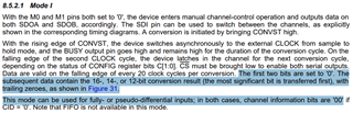
We are using ADS8363 for our application.In our schematic we didn't connect the M0 and M1(NC) Pin and our operating mode is Half clock mode(Mode-1),this configuration is correct or not?.

Is there any initial write read sequence is required to getting the output,we try to write REFDAC registers,we didn'tt get the corresponding output in the REFIO pins,and read the REFDAC registers we didn't get the expected data.

We are operating the clock at 1.85MHz.

Thanks&Regards,
Arumuga raj S

  • Hello Arumuga raj S, 

    Welcome to TI's E2E forum! 

    The M0 & M1 pins designate the channel selection mode (Manual or Automatic), and the SDO configuration (both SDOA&B or SDOA Only)

    Is there a way for the M0 & M1 pin to be shorted or connected to either ground or supply on your board/schematic? Having those pins floating could leave them in an unknown state that could lead to unknown or unreliable configurations.

    For Mode I, M0 = M1 = 0 which means they both have to be connected to GND or a logic 0 from a digital controller. This is a manual mode with both SDOA & SDOB outputting data. In this mode, for Half-Clock Mode, register bits C[1:0] have to be set for channel selection and & R[1:0] kept at "00" or "11" if no configuration is needed during data output. 

    There is a sequence needed to write to the REFDAC (covered in Section 8.5.3 in datasheet): 

    1. Enable register access control: in Config register set A[3:0] to either x010b or x101b to enable write access to REFDAC1 or REFDAC2 in the next access respectively
    2. Write to REFDACx register 
      1. Enable internal reference and its path (bit 10; RPD) to its respective REFIOx pin.
      2. Set DAC values (bits [9:0]; default is 0x3FF = 2.5V)
        1. 10-bit DAC w/ 2.5V reference 
      3. For 2.5V reference: set REFDACx register to 0x3FF (this will take care of steps a&b)
    3. Repeat for other REFDAC if both will be enabled. 

    In your case if you aren't seeing the value in the REFIOx pin, then there is a good chance that RPD (bit 10 in REFDACx register)  was not set to 0. Please let me know if steps above or at least step 2.c above sets the REFDAC value on REFIO pin. 

    ** Please note that there is an option to select which REFDAC is used for each channel. By default it is REFIO1 for all channels, so in order to use REFDAC2 for any channel register REFCM needs to be configured accordingly. It also means that setting REFDAC1 can be sufficient if similar reference value is needed for all channels. 


    Is the ADS8363 in Fully-Differential configuration or is Pseudo-Differential configuration? If the latter (Pseudo) then REFCM needs to be configured as well to select the common mode source as well. 

    Best regards, 

    Yolanda

  • Hi Yolanda Gonzalez,

    Thank you for sharing data,

    I measured the voltage in M0 and M1 pin,Pin voltage as 0V,Is that ok?.

    We are operating Fully differential configuration alone(Half clock mode)

    Thanks &regards,

    Arumuga raj S

  • Hello Arumuga, 

    It is fine for the moment, but leaving it floating does not guarantee it will stay there. having them shorted to a known value would be best. 

    Are you able to write and read back from the device?

    With the steps shared before was there an output seen on the REFIO pin? 

    Best regards, 

    Yolanda

  • Hi Yolanda Gonzalez,

    Now, I able to write and read the Config register, as well as RFDAC1&2 registers. I'm also able to get the output on the REFIO pin.

    However, when I try to read the ADC data, I get incorrect value and also channel information was not available in SDOA&B pin( where CID = '0').

    Note: 1.CHA0 given input is 44mV, but i got 1.28V in SDOA pin.

              2.CHB0 given input is 266mV, but i got 55mV in SDOB pin.

    How to read the ADC Data?, What value should I keep in C1,C2,R1 and R2 in Config register when reading the ADC data.

    Kindly share the steps for how to read the ADC data.

  • Hi Yolanda Gonzalez,

    Now we connected the Ground in M0 and M1 pin,still we didn't get the actual data.

    After the GND connection we given 3 different input to ADC

    1.ADC Given input is-0.041V(CHA0) read value is-2.477V

    2.ADC Given input is-0.236V(CHB0) read value is-0.133V

    Second level Input:

    1.ADC Given input is-0.131V(CHA0) read value is-0.0664V

    2.ADC Given input is-1.128V(CHB0) read value is-0.5639V

    Third level Input:

    .ADC Given input is-0.2849V(CHA0) read value is-0.1386V

    2.ADC Given input is-1.8956V(CHB0) read value is-0.9469V

    Note: Currently, we are writing x00000h and xF0000h (Figure 31 in datasheet)as address for reading the ADC data.

    Still, we are stuck at how to read the ADC data properly.

  • Hello Arumuga, 

    Could you please share a schematic of the ADS8363?

    Can you also measure the voltage at REFIO1, REFIO2, CMA, and CMB?

    if you could also share the sequence you are using to configure the device and read back from it? 

    Just to make sure, do you mean that you have an input on the ADC of -0.041V meaning negative 41mV or is the "-" used there not part of the value?

    Also, the data output of the ADC is in binary 2s Compliment format, could you confirm the voltage values you are reading have been converted back accordingly? 

    Best regards, 

    Yolanda

  • Hi Yolanda Gonzalez,

    After the connection of M0 and M1(connected in GND) ADC working fine,

    Conversion and read write operation was working fine

    Currently, we are writing x00000h and xF0000h (Figure 31 in datasheet)as address for reading the ADC data and channel information,but channel Information was not available in read data (SDOx pin,)

    Thanks &regards,

    Arumuga Raj S

  • Hello Arumuga, 

    Correct, like in figure 31, the ADC channel will not be in the SDO output. This is because the device is in Manual mode (Mode I), where channels are set by writing to SDI then in the N+2 cycle the data for that channel should be seen at the ADC's respective SDO. The 1st 2 bits will always be "00". 

    In other modes where the channel switching is done internally by the device (M0 =1) or when only 1 SDO is used (M1 = 1) then channel identifiers are present at SDO. 

    Does the data out match the input to the ADC channels? 

    Best regards, 

    Yolanda