


Part Number: ADS8688
Tool/software:
Subject: ADS8688 SPI Random/Garbage Values with Input Voltage on All 8 Channels
Hello everyone,
I'm currently working with an ADS8688 ADC and am encountering a strange issue that I hope someone can help me with.
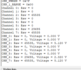
I have input voltages applied to all 8 channels of the ADS8688. However, when I try to read the conversion results via SPI, I'm consistently getting random or garbage values instead of meaningful ADC readings.
Here's some more information that might be helpful:
- ADC Part Number: ADS8688
- Problem: SPI output is random/garbage values despite valid input voltages on all 8 channels.
Could anyone offer some guidance or suggestions on what might be causing this and how to troubleshoot it?
Specifically, I'm wondering about:
- SPI Communication: Are there common pitfalls with the SPI clock, data phase/polarity (CPOL/CPHA), or chip select (CS) timing that could lead to this? My current SPI configuration is [mention].
- Power Supply: Could power supply noise or instability be a factor, even if the chip appears to be powered on?
- Grounding: Are there specific grounding considerations for the ADS8688 or my setup that I might be missing?
- Initialization/Register Configuration: Have I correctly configured all necessary registers (e.g., input range, channel enabling, reference)? I'm following the datasheet's recommended initialization sequence.
- Input Signal Integrity: While I believe my input voltages are stable, is there anything to check regarding signal integrity or over/under-range conditions that might corrupt readings?
- Code Issues: Are there any common coding errors for the ADS8688 (e.g., wrong byte order, incorrect number of bytes read) that could manifest as garbage data?

#include "ADS8688.h"
#include <stdio.h>

/*
 * INITIALISATION
 */
uint32_t ADS8688_Init(ADS8688 *ads, SPI_HandleTypeDef *spiHandle, GPIO_TypeDef *csPinBank, uint16_t csPin) {
    /* Store interface parameters in struct */
    ads->spiHandle = spiHandle;
    ads->csPinBank = csPinBank;
    ads->csPin = csPin;

    uint8_t ads_data[2] = {0};
    uint8_t state = 0;

    // Reset all registers to default
    state += ADS_Cmd_Write(ads, RST, ads_data);
    HAL_Delay(100);

    // Enable auto mode after reset
    state += ADS_Cmd_Write(ads, AUTO_RST, ads_data);
    HAL_Delay(10);

    // Enable auto transmit for all channels
    ads_data[0] = 0xFF; // Enable CH0–CH7
    state += ADS_Prog_Write(ads, AUTO_SEQ_EN, ads_data);
    HAL_Delay(10);

    // Read back for debug
    uint8_t check_data[2];
    ADS_Prog_Read(ads, AUTO_SEQ_EN, check_data);
    printf("AUTO_SEQ_EN = 0x%02X\n", check_data[0]); // Should print 0xFF

    // Power down unused channels (CH0, CH2–7)
    ads_data[0] = 0xFD; // Power down CH0, CH2–7 (1 = powered down, CH1 active)
    state += ADS_Prog_Write(ads, CHN_PWRDN, ads_data);
    HAL_Delay(10);

    // Read back for debug
    ADS_Prog_Read(ads, CHN_PWRDN, check_data);
    printf("CHN_PWRDN = 0x%02X\n", check_data[0]); // Should print 0xFD

    // Set desired features
    ads_data[0] = 0x03; // Default feature select
    state += ADS_Prog_Write(ads, FEATURE_SELECT, ads_data);
    HAL_Delay(10);

    // Set input ranges (all channels: ±2.56 V for consistency)
    ads_data[0] = 0x06; state += ADS_Prog_Write(ads, CHN_0_RANGE, ads_data); HAL_Delay(10);
    ads_data[0] = 0x06; state += ADS_Prog_Write(ads, CHN_1_RANGE, ads_data); HAL_Delay(10);
    ads_data[0] = 0x06; state += ADS_Prog_Write(ads, CHN_2_RANGE, ads_data); HAL_Delay(10);
    ads_data[0] = 0x06; state += ADS_Prog_Write(ads, CHN_3_RANGE, ads_data); HAL_Delay(10);
    ads_data[0] = 0x06; state += ADS_Prog_Write(ads, CHN_4_RANGE, ads_data); HAL_Delay(10);
    ads_data[0] = 0x06; state += ADS_Prog_Write(ads, CHN_5_RANGE, ads_data); HAL_Delay(10);
    ads_data[0] = 0x06; state += ADS_Prog_Write(ads, CHN_6_RANGE, ads_data); HAL_Delay(10);
    ads_data[0] = 0x06; state += ADS_Prog_Write(ads, CHN_7_RANGE, ads_data); HAL_Delay(10);

    // Read back Channel 1 range for debug
    ADS_Prog_Read(ads, CHN_1_RANGE, check_data);
    printf("CHN_1_RANGE = 0x%02X\n", check_data[0]); // Should print 0x06

    return state;
}

/*
 * REGISTER ACCESS FUNCTIONS
 */
HAL_StatusTypeDef ADS_Prog_Read(ADS8688 *ads, uint8_t addr, uint8_t *data) {
    HAL_StatusTypeDef ret;
    uint16_t txbuf[1] = {((addr << 1) & 0xFE) << 8};
    uint16_t rxbuf[1];

    HAL_GPIO_WritePin(ads->csPinBank, ads->csPin, GPIO_PIN_RESET);
    ret = HAL_SPI_TransmitReceive(ads->spiHandle, (uint8_t *)txbuf, (uint8_t *)rxbuf, 1, 10);
    HAL_GPIO_WritePin(ads->csPinBank, ads->csPin, GPIO_PIN_SET);

    data[0] = (rxbuf[0] >> 8) & 0xFF;
    data[1] = rxbuf[0] & 0xFF;
    return ret;
}

HAL_StatusTypeDef ADS_Prog_Write(ADS8688 *ads, uint8_t addr, uint8_t *data) {
    HAL_StatusTypeDef ret;
    uint16_t txbuf[1] = {((addr << 1) | 0x01) << 8 | data[0]};
    uint16_t rxbuf[1];

    HAL_GPIO_WritePin(ads->csPinBank, ads->csPin, GPIO_PIN_RESET);
    ret = HAL_SPI_TransmitReceive(ads->spiHandle, (uint8_t *)txbuf, (uint8_t *)rxbuf, 1, 10);
    HAL_GPIO_WritePin(ads->csPinBank, ads->csPin, GPIO_PIN_SET);

    data[0] = rxbuf[0] & 0xFF;
    data[1] = 0;
    return ret;
}

HAL_StatusTypeDef ADS_Cmd_Write(ADS8688 *ads, uint8_t cmd, uint8_t *data) {
    HAL_StatusTypeDef ret;
    uint16_t txbuf[1] = {cmd << 8};
    uint16_t rxbuf[1];

    HAL_GPIO_WritePin(ads->csPinBank, ads->csPin, GPIO_PIN_RESET);
    ret = HAL_SPI_TransmitReceive(ads->spiHandle, (uint8_t *)txbuf, (uint8_t *)rxbuf, 1, 10);
    HAL_GPIO_WritePin(ads->csPinBank, ads->csPin, GPIO_PIN_SET);

    data[0] = (rxbuf[0] >> 8) & 0xFF;
    data[1] = rxbuf[0] & 0xFF;
    return ret;
}

/*
 * READ ALL CHANNELS (AUTO MODE)
 */
HAL_StatusTypeDef ADS_Read_All_Raw(ADS8688 *ads, uint16_t *data) {
    HAL_StatusTypeDef ret = HAL_OK;
    uint16_t txbuf[1] = { CONT << 8 }; // Continue command (0x00)
    uint16_t rxbuf[1];

    for (int i = 0; i < CHNS_NUM_READ; i++) {
        // Pull CS low to start SPI transaction
        HAL_GPIO_WritePin(ads->csPinBank, ads->csPin, GPIO_PIN_RESET);

        // Send CONT command and receive data
        ret = HAL_SPI_TransmitReceive(
            ads->spiHandle,
            (uint8_t *)txbuf,
            (uint8_t *)rxbuf,
            sizeof(txbuf),
            100
        );

        // Pull CS high to end SPI transaction
        HAL_GPIO_WritePin(ads->csPinBank, ads->csPin, GPIO_PIN_SET);

        if (ret != HAL_OK) {
            printf("SPI Error on channel %d\r\n", i);
            return ret;
        }

        // Store the 16-bit raw ADC value
        data[i] = rxbuf[0];
        printf("Channel %d: Raw = %u\n", i, data[i]); // Debug print

        HAL_Delay(1); // Small delay for stability
    }

    return HAL_OK;
}
/* USER CODE BEGIN Header */
/**
  ******************************************************************************
  * @file           : main.c
  * @brief          : Main program body
  ******************************************************************************
  * @attention
  *
  * Copyright (c) 2025 STMicroelectronics.
  * All rights reserved.
  *
  * This software is licensed under terms that can be found in the LICENSE file
  * in the root directory of this software component.
  * If no LICENSE file comes with this software, it is provided AS-IS.
  *
  ******************************************************************************
  */
/* USER CODE END Header */
/* Includes ------------------------------------------------------------------*/
#include "main.h"
#include "ADS8688.h"
#include <stdio.h>
#include <string.h>
/* Private includes ----------------------------------------------------------*/
/* USER CODE BEGIN Includes */
#define default_interval 500
/* USER CODE END Includes */

/* Private typedef -----------------------------------------------------------*/
/* USER CODE BEGIN PTD */
unsigned int current = 0, previous = 0, interval = default_interval;
/* USER CODE END PTD */

/* Private define ------------------------------------------------------------*/
/* USER CODE BEGIN PD */
ADS8688 ads;
uint16_t ads_data[8]; // All 8 channels
float volt_helper = 0;
/* USER CODE END PD */

/* Private macro -------------------------------------------------------------*/
/* USER CODE BEGIN PM */

/* USER CODE END PM */

/* Private variables ---------------------------------------------------------*/
SPI_HandleTypeDef hspi3;

UART_HandleTypeDef huart4;

/* USER CODE BEGIN PV */

/* USER CODE END PV */

/* Private function prototypes -----------------------------------------------*/
void SystemClock_Config(void);
static void MX_GPIO_Init(void);
static void MX_SPI3_Init(void);
static void MX_UART4_Init(void);
/* USER CODE BEGIN PFP */
int __io_putchar(int ch)
{
    HAL_UART_Transmit(&huart4, (uint8_t *)&ch, 1, 100); // 100 ms timeout
    return ch;
}
/* USER CODE END PFP */

/* Private user code ---------------------------------------------------------*/
/* USER CODE BEGIN 0 */

/* USER CODE END 0 */

/**
  * @brief  The application entry point.
  * @retval int
  */
int main(void)
{
  /* USER CODE BEGIN 1 */

  /* USER CODE END 1 */

  /* MCU Configuration--------------------------------------------------------*/

  /* Reset of all peripherals, Initializes the Flash interface and the Systick. */
  HAL_Init();

  /* USER CODE BEGIN Init */

  /* USER CODE END Init */

  /* Configure the system clock */
  SystemClock_Config();

  /* USER CODE BEGIN SysInit */

  /* USER CODE END SysInit */

  /* Initialize all configured peripherals */
  MX_GPIO_Init();
  MX_SPI3_Init();
  MX_UART4_Init();
  /* USER CODE BEGIN 2 */
  printf("UART Test\n"); // Debug print to confirm UART
      HAL_GPIO_WritePin(GPIOA, GPIO_PIN_15, GPIO_PIN_SET);
      if (ADS8688_Init(&ads, &hspi3, GPIOA, GPIO_PIN_15) != 0) {
          printf("ADS8688 Initialization Failed\n");
          Error_Handler();
      }
  /* USER CODE END 2 */

  /* Infinite loop */
  /* USER CODE BEGIN WHILE */
  while (1)
  {
    /* USER CODE END WHILE */
	  current = HAL_GetTick();
	          if (current >= previous + interval) {
	              // Read all 8 channels
	              if (ADS_Read_All_Raw(&ads, ads_data) != HAL_OK) {
	                  printf("Error reading ADS8688 data\n");
	                  previous = current;
	                  continue;
	              }

	              // Process and print data for each channel
	              char output[512];
	              int len = 0;
	              for (int i = 0; i < 8; i++) {
	                  volt_helper = ((float)ads_data[i]) * 4.098f / 65535.0f; // ±2.56 V range
	                  len += snprintf(output + len, sizeof(output) - len,
	                                  "CHN_%d: Raw = %u, Voltage = %.3f V\n", i, ads_data[i], volt_helper);
	              }
	              HAL_UART_Transmit(&huart4, (uint8_t *)output, len, 100);

	              previous = current;
	              break ;
	          }
	          /* USER CODE BEGIN 3 */
	      }
	      /* USER CODE END 3
	      /* USER CODE END 3 */
	  }

	  /**
	    * @brief System Clock Configuration
	    * @retval None
	    */

  /* USER CODE END 3 */


/**
  * @brief System Clock Configuration
  * @retval None
  */
void SystemClock_Config(void)
{
  RCC_OscInitTypeDef RCC_OscInitStruct = {0};
  RCC_ClkInitTypeDef RCC_ClkInitStruct = {0};

  /** Configure the main internal regulator output voltage
  */
  __HAL_RCC_PWR_CLK_ENABLE();
  __HAL_PWR_VOLTAGESCALING_CONFIG(PWR_REGULATOR_VOLTAGE_SCALE3);

  /** Initializes the RCC Oscillators according to the specified parameters
  * in the RCC_OscInitTypeDef structure.
  */
  RCC_OscInitStruct.OscillatorType = RCC_OSCILLATORTYPE_HSI;
  RCC_OscInitStruct.HSIState = RCC_HSI_ON;
  RCC_OscInitStruct.HSICalibrationValue = RCC_HSICALIBRATION_DEFAULT;
  RCC_OscInitStruct.PLL.PLLState = RCC_PLL_NONE;
  if (HAL_RCC_OscConfig(&RCC_OscInitStruct) != HAL_OK)
  {
    Error_Handler();
  }

  /** Initializes the CPU, AHB and APB buses clocks
  */
  RCC_ClkInitStruct.ClockType = RCC_CLOCKTYPE_HCLK|RCC_CLOCKTYPE_SYSCLK
                              |RCC_CLOCKTYPE_PCLK1|RCC_CLOCKTYPE_PCLK2;
  RCC_ClkInitStruct.SYSCLKSource = RCC_SYSCLKSOURCE_HSI;
  RCC_ClkInitStruct.AHBCLKDivider = RCC_SYSCLK_DIV1;
  RCC_ClkInitStruct.APB1CLKDivider = RCC_HCLK_DIV1;
  RCC_ClkInitStruct.APB2CLKDivider = RCC_HCLK_DIV1;

  if (HAL_RCC_ClockConfig(&RCC_ClkInitStruct, FLASH_LATENCY_0) != HAL_OK)
  {
    Error_Handler();
  }
}

/**
  * @brief SPI3 Initialization Function
  * @param None
  * @retval None
  */
static void MX_SPI3_Init(void)
{

  /* USER CODE BEGIN SPI3_Init 0 */

  /* USER CODE END SPI3_Init 0 */

  /* USER CODE BEGIN SPI3_Init 1 */

  /* USER CODE END SPI3_Init 1 */
  /* SPI3 parameter configuration*/
  hspi3.Instance = SPI3;
  hspi3.Init.Mode = SPI_MODE_MASTER;
  hspi3.Init.Direction = SPI_DIRECTION_2LINES;
  hspi3.Init.DataSize = SPI_DATASIZE_16BIT;
  hspi3.Init.CLKPolarity = SPI_POLARITY_LOW;
  hspi3.Init.CLKPhase = SPI_PHASE_1EDGE;
  hspi3.Init.NSS = SPI_NSS_SOFT;
  hspi3.Init.BaudRatePrescaler = SPI_BAUDRATEPRESCALER_16;
  hspi3.Init.FirstBit = SPI_FIRSTBIT_MSB;
  hspi3.Init.TIMode = SPI_TIMODE_DISABLE;
  hspi3.Init.CRCCalculation = SPI_CRCCALCULATION_DISABLE;
  hspi3.Init.CRCPolynomial = 10;
  if (HAL_SPI_Init(&hspi3) != HAL_OK)
  {
    Error_Handler();
  }
  /* USER CODE BEGIN SPI3_Init 2 */

  /* USER CODE END SPI3_Init 2 */

}

/**
  * @brief UART4 Initialization Function
  * @param None
  * @retval None
  */
static void MX_UART4_Init(void)
{

  /* USER CODE BEGIN UART4_Init 0 */

  /* USER CODE END UART4_Init 0 */

  /* USER CODE BEGIN UART4_Init 1 */

  /* USER CODE END UART4_Init 1 */
  huart4.Instance = UART4;
  huart4.Init.BaudRate = 115200;
  huart4.Init.WordLength = UART_WORDLENGTH_8B;
  huart4.Init.StopBits = UART_STOPBITS_1;
  huart4.Init.Parity = UART_PARITY_NONE;
  huart4.Init.Mode = UART_MODE_TX_RX;
  huart4.Init.HwFlowCtl = UART_HWCONTROL_NONE;
  huart4.Init.OverSampling = UART_OVERSAMPLING_16;
  if (HAL_UART_Init(&huart4) != HAL_OK)
  {
    Error_Handler();
  }
  /* USER CODE BEGIN UART4_Init 2 */

  /* USER CODE END UART4_Init 2 */

}

/**
  * @brief GPIO Initialization Function
  * @param None
  * @retval None
  */
static void MX_GPIO_Init(void)
{
  GPIO_InitTypeDef GPIO_InitStruct = {0};
/* USER CODE BEGIN MX_GPIO_Init_1 */
/* USER CODE END MX_GPIO_Init_1 */

  /* GPIO Ports Clock Enable */
  __HAL_RCC_GPIOC_CLK_ENABLE();
  __HAL_RCC_GPIOA_CLK_ENABLE();

  /*Configure GPIO pin Output Level */
  HAL_GPIO_WritePin(GPIOA, GPIO_PIN_15, GPIO_PIN_RESET);

  /*Configure GPIO pin : PA15 */
  GPIO_InitStruct.Pin = GPIO_PIN_15;
  GPIO_InitStruct.Mode = GPIO_MODE_OUTPUT_PP;
  GPIO_InitStruct.Pull = GPIO_NOPULL;
  GPIO_InitStruct.Speed = GPIO_SPEED_FREQ_VERY_HIGH;
  HAL_GPIO_Init(GPIOA, &GPIO_InitStruct);

/* USER CODE BEGIN MX_GPIO_Init_2 */
/* USER CODE END MX_GPIO_Init_2 */
}

/* USER CODE BEGIN 4 */

/* USER CODE END 4 */

/**
  * @brief  This function is executed in case of error occurrence.
  * @retval None
  */
void Error_Handler(void)
{
  /* USER CODE BEGIN Error_Handler_Debug */
  /* User can add his own implementation to report the HAL error return state */
  __disable_irq();
  while (1)
  {
  }
  /* USER CODE END Error_Handler_Debug */
}

#ifdef  USE_FULL_ASSERT
/**
  * @brief  Reports the name of the source file and the source line number
  *         where the assert_param error has occurred.
  * @param  file: pointer to the source file name
  * @param  line: assert_param error line source number
  * @retval None
  */
void assert_failed(uint8_t *file, uint32_t line)
{
  /* USER CODE BEGIN 6 */
  /* User can add his own implementation to report the file name and line number,
     ex: printf("Wrong parameters value: file %s on line %d\r\n", file, line) */
  /* USER CODE END 6 */
}
#endif /* USE_FULL_ASSERT */

