This thread has been locked.

If you have a related question, please click the "Ask a related question" button in the top right corner. The newly created question will be automatically linked to this question.

ADS131B04-Q1: ADC output data is inaccurate

Part Number: ADS131B04-Q1

Tool/software:

Dear Experts,

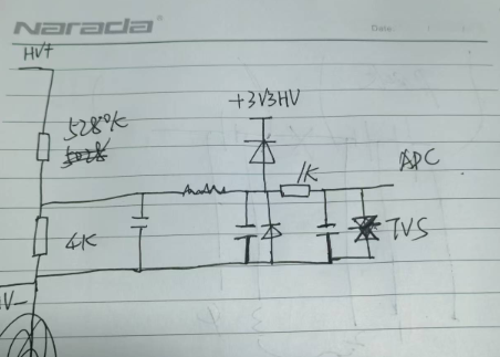
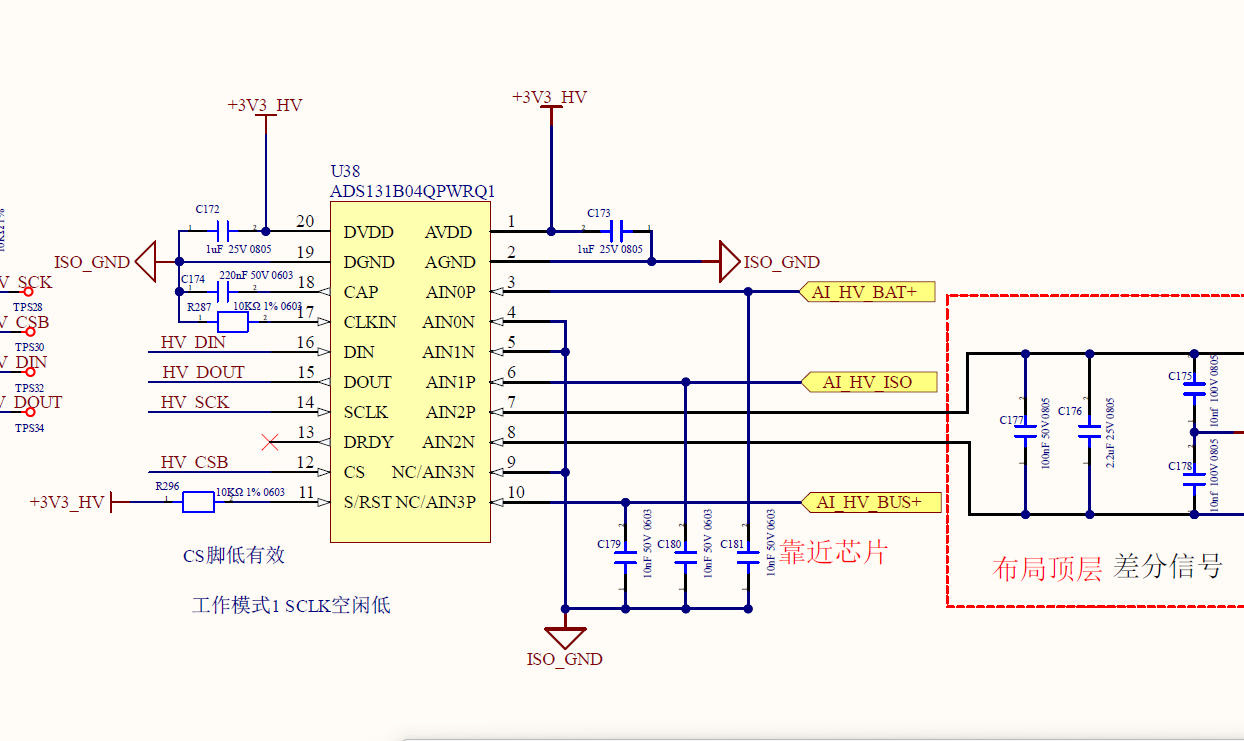
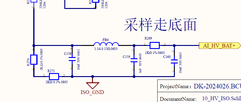
At present, our product is experiencing an abnormal phenomenon during pulse and electrostatic testing. The bus voltage is 200V, and after passing through the peripheral voltage divider circuit, the input ADC AIN0 voltage is 0.1514V.

However, during pulse and electrostatic testing, the input ADC voltage is still stable at 0.1514V. The upper computer displays that the ADC measurement output has changed to 159V. After the circuit is powered off and restarted, the output returns to normal 200V. When tested again, the fault will recur;

When a fault occurs, we change the bus voltage to 100V, and the output voltage will also change to 79.5V. This phenomenon is very strange, and we would like to ask an expert what the cause of this fault is. Currently, The fault occurred at input port A0, while other ports are normal. It is possible that other ports may also exist, but it has not been discovered yet. The ADC gain is 1, and the circuit peripheral diagram is shown below. Please help analyze it. Thank you very much

  • Hi Colln,

    Is the pulse and electrostatic testing you mentioned a standard IEC testing (e.g. EFT, surge etc.)? Is the V- in your image connected to a ground or a DC voltage? Did you monitor the conversion data from the ADC to see if they match the data that are displayed on the upper computer?

    BR,

    Dale

  • Hi Dale,

    The testing standard is in accordance with GB/T 34131, HV - is GND; At present, we are unable to directly read ADC conversion data for our product, and can only read the final conversion result; We suspect that the reason may be due to electrostatic testing affecting the conversion of this ADC chip, or it may be due to the design of the analog input peripheral circuit. Regarding the design of the analog input circuit for this chip, what is the maximum value of the current limiting resistor for the input port? How should the filtering circuit be designed? Please provide some suggestions,thank you

  • Hi Colin Chen,

    Dale is out of the office today, please expect a response next week. Thanks for your patience

    -Bryan

  • Hi Colin,

    This kind of the test is really related to the system design, not only the circuit design but also the PCB layout design. There are a lot of rules the customer has to follow. For example, this ADC can support positive and negative input signal which is lower than the ground. If the customer measures the bidirectional current, the input signal could be negative, so the protection diodes in your image is not a proper design, see Circuit for protecting ADS131M0x ADC from electrical overstress. Also, the +3V3HV supply should be properly protected to conduct the fault current to the ground. 

    The current limiting resistor is not determined by the ADC, it is a system consideration. The bigger value of the current limiting resistor, the better protection to the ADC, but the bigger value of the current limiting resistor can also contribute more errors including the offset error when the leakage current is flowing through it and also the gain error.

    The PCB layout is also important for passing such testing.

    BR,

    Dale

  • Hi Dale,

    At present, we have made modifications to the peripheral circuit based on the documentation, but the test still results in output errors. Sometimes it also causes changes in the voltage of the input ADC port. It feels like when the chip is subjected to pulse or electrostatic testing, it can cause an abnormality in a certain part of the ADC chip, resulting in output failure; After powering down and restarting, the chip will return to normal.Replacing the ADC chip for testing may also result in the same issue.

    In most test scenarios, the actual voltage is higher than the voltage sampled by the ADC. The input voltage to the ADC is normal, but the sampled output voltage is abnormal.

    Please help to analyze the reasons again and provide solutions. Thank you

  • Hi Colin,

    Can you let me know how the customer modified their circuit? What's the test signal level and frequency? As I said, this kind of test is highly related to the system design, it is impossible to expect the ADC to stand all the transient signals, the protection circuity can help to protect the ADC from the the transient signals, but it can not be guaranteed. The PCB layout is also important for passing such testing. I can check and share my suggestions if the customer can share the schematic and pcb layout files (not the screenshots or a simple circuit like you shared). 

    BR,

    Dale

  • Hi Dale,

    The customer's schematic diagram is as follows.

    We noticed that the DRDY pin is not connected or pulled up by 100K Ω to the DVDD when not in use. Today, we pulled up the DRDY pin by 100K Ω and found that the test was normal; Is it possible that the output abnormality is caused by the tube foot not being pulled up? According to our understanding, this is a state output pin. Will it affect the ADC conversion output? How does it affect? Thank you~

  • Hi Colin,

    /DRDY is an output signal to indicate whether the data is ready or not. We always recommend to use this signal to retrieve the conversion data because you could read the previous data if you miss reading the data in the past frames. If you read the data in a certain time interval, you could mess up and miss reading the data because the clock can be shifting. The synchronization signal can help to minimize the impact but you are not using the /SYNC on pin 11.

    BR,

    Dale