This thread has been locked.

If you have a related question, please click the "Ask a related question" button in the top right corner. The newly created question will be automatically linked to this question.

ADS1158: ADS1158 Single Channel Reading not happening!

Part Number: ADS1158

Tool/software:

Hi,

I am unable to read the Data in the ADC channel in the Fixed Channel mode, data is incorrect.


I am applying 0.5V to the Input channel for Channel o, the value is not corresponding to the 0.5V.


Kindly guide me  any configuration issue or the Reading method is wrong here.


For the benefit of quick understating and I feel Channel Selection and the specifying the Channel for reading is wrong, but I am not sure, can you put some light on it.


It would be great help, if I find solution here.Thanks in advance.
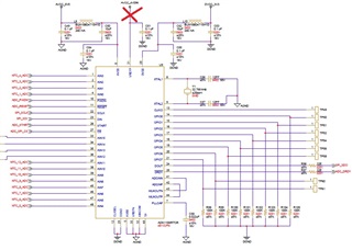
Connection

PWDN & RESET - Pin Pulled Up with 3.3V with 100k

AVDD - +5V


VREFP - Configured for internal Reference in the Software

VREFN - DGND//No need connection if I make internal reference?


AVSS,VREFN,AINCOM - GND


CLKSEL - Not Connected


XTAL1- XTAL2 - 32.768kHz Crystal Connection//Default Connection in the ADS1258EVM Board


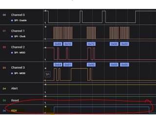
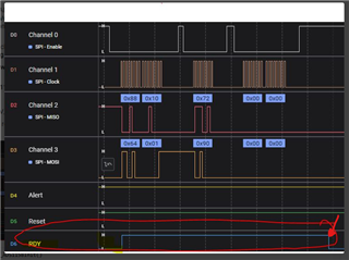
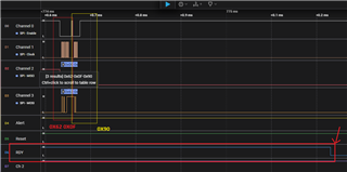
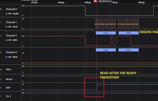
DRDY - Controller General Purpose input//Made to monitor the Pin READY up on Data ready


SPI Connection - Standard Connection with the Microcontroller


//Software Configuration

SPI - MODE 0,1Mhz


//Registry Configuration

#define DAQ_DRV_REG_ADDR_CONFIG0                    ((uint8_t) 0x00)
#define DAQ_DRV_REG_ADDR_CONFIG1                    ((uint8_t) 0x01)
#define DAQ_DRV_REG_ADDR_MUXSCH                     ((uint8_t) 0x02)
#define DAQ_DRV_REG_ADDR_MUXDIF                     ((uint8_t) 0x03)
#define DAQ_DRV_REG_ADDR_MUXSG0                     ((uint8_t) 0x04)
#define DAQ_DRV_REG_ADDR_MUXSG1                     ((uint8_t) 0x05)
#define DAQ_DRV_REG_ADDR_SYSRED                     ((uint8_t) 0x06)

#define DAQ_DRV_OPCODE_READ_DIRECT			        ((uint8_t) 0x00)
#define DAQ_DRV_OPCODE_READ_COMMAND			        ((uint8_t) 0x30)    // Includes MUL bit
#define DAQ_DRV_OPCODE_RREG							((uint8_t) 0x40)
#define DAQ_DRV_OPCODE_WREG							((uint8_t) 0x60)
#define DAQ_DRV_OPCODE_PULSE_CONVERT		        ((uint8_t) 0x80)
#define DAQ_DRV_OPCODE_RESET						((uint8_t) 0xC0)
    
    /* Commands byte masks */
    #define DAQ_DRV_OPCODE_C_MASK                       ((uint8_t) 0xE0)
    #define DAQ_DRV_OPCODE_MUL_MASK                     ((uint8_t) 0x10)
    #define DAQ_DRV_OPCODE_A_MASK                       ((uint8_t) 0x0F)    

static void daq_drv_ADS1158Init()
{
    // Want to configure the Internal Reference for the Voltage, Single ended ADC, want to read all 16 channels one after the other once ADC read command triggered and Ready pin goes low and High,indicating Ready tor ead the Data

    uint8_t l_ucRegDataArray[10];

    l_ucRegDataArray[DAQ_DRV_REG_ADDR_CONFIG0]   =   0b00100000;//Fixed Channel Mode,Rest all Disabled(SPIRST,

    
    l_ucRegDataArray[DAQ_DRV_REG_ADDR_CONFIG1]   =   0;
    l_ucRegDataArray[DAQ_DRV_REG_ADDR_MUXSCH]    =   0xFF;//Not sure , this should be enabled, no proper description in the datasheet
    l_ucRegDataArray[DAQ_DRV_REG_ADDR_MUXDIF]    =   0;//Since its not diffrention ADC to be read
    l_ucRegDataArray[DAQ_DRV_REG_ADDR_MUXSG0]    =   0;//Initially diasbled
    l_ucRegDataArray[DAQ_DRV_REG_ADDR_MUXSG1]    =   0;//Initially diasbled
    l_ucRegDataArray[DAQ_DRV_REG_ADDR_SYSRED]    =   0b00100000;//Internal Reference for the ADC is Enabled
 
    // SInce GPIO's are not used Not configured for any pins
   daq_drv_WriteMultipleRegisters(0, 7,l_ucRegDataArray);// For to Write Multiple registry 

}
static void daq_drv_WriteMultipleRegisters(uint8_t startAddress, uint8_t count, const uint8_t *regData)
{
    s_ucDataTx[0] = DAQ_DRV_OPCODE_WREG | DAQ_DRV_OPCODE_MUL_MASK | (startAddress & DAQ_DRV_OPCODE_A_MASK);
    memcpy(&s_ucDataTx[1],regData,count);//Copy the dat for Writing Multiple registries

    daq_drv_SpiTxRx(DAQ_DRV_SPI_ADS1158_DEVICE_IDX,s_ucDataTx,s_ucDataRx,(1 + count));//Transmit through SPI
}

static int32_t daq_drv_AdcRead(uint8_t l_ucAdcChId, uint8_t l_ucTimeoutVal)
{
    uint8_t l_ucRdyStatus;
    unsigned long runningms;
    static uint8_t s_ucRegistrySwitched;

    //Select Channel 
    if(l_ucAdcChId < 8)
    {
      if( s_ucRegistrySwitched )
      {
        // Clear the DAQ_DRV_REG_ADDR_MUXSG1
        s_ucDataTx[0] = DAQ_DRV_OPCODE_WREG | (DAQ_DRV_REG_ADDR_MUXSG1 & DAQ_DRV_OPCODE_A_MASK);
        s_ucDataTx[1] =  0;//Clear the Previous Selection of Registry
        /* Initiate transfer */
        daq_drv_SpiTxRx(DAQ_DRV_SPI_ADS1158_DEVICE_IDX,s_ucDataTx,s_ucDataRx,2);
        s_ucRegistrySwitched = 0;
      }
      s_ucDataTx[0] = DAQ_DRV_OPCODE_WREG | (DAQ_DRV_REG_ADDR_MUXSG0 & DAQ_DRV_OPCODE_A_MASK);
      s_ucDataTx[1] =  (1 << l_ucAdcChId);

      /* Initiate transfer */
      daq_drv_SpiTxRx(DAQ_DRV_SPI_ADS1158_DEVICE_IDX,s_ucDataTx,s_ucDataRx,2);
    }
    else
    {
      if( s_ucRegistrySwitched == 0 )
      {
        // Clear the DAQ_DRV_REG_ADDR_MUXSG0
        s_ucDataTx[0] = DAQ_DRV_OPCODE_WREG | (DAQ_DRV_REG_ADDR_MUXSG0 & DAQ_DRV_OPCODE_A_MASK);
        s_ucDataTx[1] =  0;//Clear the Previous Selection of Registry
        /* Initiate transfer */
        daq_drv_SpiTxRx(DAQ_DRV_SPI_ADS1158_DEVICE_IDX,s_ucDataTx,s_ucDataRx,2);
        s_ucRegistrySwitched = 1;
      }
      s_ucDataTx[0] = DAQ_DRV_OPCODE_WREG | (DAQ_DRV_REG_ADDR_MUXSG1 & DAQ_DRV_OPCODE_A_MASK);
      s_ucDataTx[1] =  (1 << (l_ucAdcChId % 8) );

      /* Initiate transfer */
      daq_drv_SpiTxRx(DAQ_DRV_SPI_ADS1158_DEVICE_IDX,s_ucDataTx,s_ucDataRx,2);      
    }

    s_ucDataTx[0] = DAQ_DRV_OPCODE_PULSE_CONVERT| DAQ_DRV_OPCODE_MUL_MASK;

    daq_drv_SpiTxRx(DAQ_DRV_SPI_ADS1158_DEVICE_IDX,s_ucDataTx,s_ucDataTx,1);

    runningms = xTaskGetTickCount();
    l_ucRdyStatus=daq_drv_GPIOGet(s_stGPIOMappings,0);//Check ADC_DRDY_PIN 
    while( l_ucRdyStatus )
    {
      l_ucRdyStatus=daq_drv_GPIOGet(s_stGPIOMappings,0);

      if( (runningms + l_ucTimeoutVal) < xTaskGetTickCount() )
      {
        return ADC_ERROR;//Error state
      }
    }

    // Dummy bytes for reading the Data
    s_ucDataTx[0] = 0;
    s_ucDataTx[1] = 0;

    daq_drv_SpiTxRx(DAQ_DRV_SPI_ADS1158_DEVICE_IDX,s_ucDataTx,s_ucDataRx,2);

    //printf("\nD:%d",((s_ucSpiDataRx[0] << 8) | s_ucSpiDataRx[1]));

    return ((s_ucDataRx[0] << 8) | s_ucDataRx[1]);  
}

void main()
{
    unsigned char l_ucChannel = 0;
    InitDevice();
    InitSpi();//SPI - MODE 0,1Mhz
    daq_drv_ADS1158Init();
    
    while(1)
    {
        
        printf("\n ADC: %d",daq_drv_AdcRead(l_ucChannel, 100));
        
        l_ucChannel ++;
        if(l_ucChannel>15)
            l_ucChannel = 0;
        
            
    }

}

  • Hi Bharadwaj M N,

    Can you please provide a schematic of your system as well as logic analyzer captures showing the communication? Please include all relevant SPI signals (CS, SCLK, DOUT, DIN, DRDY)

    -Bryan

  • HI ,

    Thanks for the response.

    I am using the Eval board of ADS1158,Please find the https://mm.digikey.com/Volume0/opasdata/d220001/medias/docus/2208/ADS1158EVM_1258EVM_-PDK_Gde.pdf (Eval board Please follow Page 37), rest all configuration as mentioned above, since It has so many jumper configuration, above I have explained the connection, if any thing more kindly let me know.

    Also kindly find the code, which is mainly consist of Configuration of Registry and the Reading of ADC, in which I have doubt on my Registry configuration and the Reading of the ADC Channels which seems to be incorrect.

    Also kindly find the attached waveform of the Command and response.(I have connected 1.6V to ADC Channel 0), always get the read response of 0.

    Read Command  0x64 // 0b01100100  (011 - Registry Write Command)  (0 - No multiple registry)  ( 0100- Registry 4 Selected) 

    Channel Selction - 0x01

    Followed By 0x90, //DAQ_DRV_OPCODE_PULSE_CONVERT| DAQ_DRV_OPCODE_MUL_MASK;

    Followed by Dummy bytes to read the registry 0x00,0x00 to ready 2 bytes of data

    //Registry Configuration
    
    #define DAQ_DRV_REG_ADDR_CONFIG0                    ((uint8_t) 0x00)
    #define DAQ_DRV_REG_ADDR_CONFIG1                    ((uint8_t) 0x01)
    #define DAQ_DRV_REG_ADDR_MUXSCH                     ((uint8_t) 0x02)
    #define DAQ_DRV_REG_ADDR_MUXDIF                     ((uint8_t) 0x03)
    #define DAQ_DRV_REG_ADDR_MUXSG0                     ((uint8_t) 0x04)
    #define DAQ_DRV_REG_ADDR_MUXSG1                     ((uint8_t) 0x05)
    #define DAQ_DRV_REG_ADDR_SYSRED                     ((uint8_t) 0x06)
    
    #define DAQ_DRV_OPCODE_READ_DIRECT			        ((uint8_t) 0x00)
    #define DAQ_DRV_OPCODE_READ_COMMAND			        ((uint8_t) 0x30)    // Includes MUL bit
    #define DAQ_DRV_OPCODE_RREG							((uint8_t) 0x40)
    #define DAQ_DRV_OPCODE_WREG							((uint8_t) 0x60)
    #define DAQ_DRV_OPCODE_PULSE_CONVERT		        ((uint8_t) 0x80)
    #define DAQ_DRV_OPCODE_RESET						((uint8_t) 0xC0)
        
        /* Commands byte masks */
        #define DAQ_DRV_OPCODE_C_MASK                       ((uint8_t) 0xE0)
        #define DAQ_DRV_OPCODE_MUL_MASK                     ((uint8_t) 0x10)
        #define DAQ_DRV_OPCODE_A_MASK                       ((uint8_t) 0x0F)    
    
    static void daq_drv_ADS1158Init()
    {
        // Want to configure the Internal Reference for the Voltage, Single ended ADC, want to read all 16 channels one after the other once ADC read command triggered and Ready pin goes low and High,indicating Ready tor ead the Data
    
        uint8_t l_ucRegDataArray[10];
    
        l_ucRegDataArray[DAQ_DRV_REG_ADDR_CONFIG0]   =   0b00100000;//Fixed Channel Mode,Rest all Disabled(SPIRST,
    
        
        l_ucRegDataArray[DAQ_DRV_REG_ADDR_CONFIG1]   =   0;
        l_ucRegDataArray[DAQ_DRV_REG_ADDR_MUXSCH]    =   0xFF;//Not sure , this should be enabled, no proper description in the datasheet
        l_ucRegDataArray[DAQ_DRV_REG_ADDR_MUXDIF]    =   0;//Since its not diffrention ADC to be read
        l_ucRegDataArray[DAQ_DRV_REG_ADDR_MUXSG0]    =   0;//Initially diasbled
        l_ucRegDataArray[DAQ_DRV_REG_ADDR_MUXSG1]    =   0;//Initially diasbled
        l_ucRegDataArray[DAQ_DRV_REG_ADDR_SYSRED]    =   0b00100000;//Internal Reference for the ADC is Enabled
     
        // SInce GPIO's are not used Not configured for any pins
       daq_drv_WriteMultipleRegisters(0, 7,l_ucRegDataArray);// For to Write Multiple registry 
    
    }
    static void daq_drv_WriteMultipleRegisters(uint8_t startAddress, uint8_t count, const uint8_t *regData)
    {
        s_ucDataTx[0] = DAQ_DRV_OPCODE_WREG | DAQ_DRV_OPCODE_MUL_MASK | (startAddress & DAQ_DRV_OPCODE_A_MASK);
        memcpy(&s_ucDataTx[1],regData,count);//Copy the dat for Writing Multiple registries
    
        daq_drv_SpiTxRx(DAQ_DRV_SPI_ADS1158_DEVICE_IDX,s_ucDataTx,s_ucDataRx,(1 + count));//Transmit through SPI
    }
    
    static int32_t daq_drv_AdcRead(uint8_t l_ucAdcChId, uint8_t l_ucTimeoutVal)
    {
        uint8_t l_ucRdyStatus;
        unsigned long runningms;
        static uint8_t s_ucRegistrySwitched;
    
        //Select Channel 
        if(l_ucAdcChId < 8)
        {
          if( s_ucRegistrySwitched )
          {
            // Clear the DAQ_DRV_REG_ADDR_MUXSG1
            s_ucDataTx[0] = DAQ_DRV_OPCODE_WREG | (DAQ_DRV_REG_ADDR_MUXSG1 & DAQ_DRV_OPCODE_A_MASK);
            s_ucDataTx[1] =  0;//Clear the Previous Selection of Registry
            /* Initiate transfer */
            daq_drv_SpiTxRx(DAQ_DRV_SPI_ADS1158_DEVICE_IDX,s_ucDataTx,s_ucDataRx,2);
            s_ucRegistrySwitched = 0;
          }
          s_ucDataTx[0] = DAQ_DRV_OPCODE_WREG | (DAQ_DRV_REG_ADDR_MUXSG0 & DAQ_DRV_OPCODE_A_MASK);
          s_ucDataTx[1] =  (1 << l_ucAdcChId);
    
          /* Initiate transfer */
          daq_drv_SpiTxRx(DAQ_DRV_SPI_ADS1158_DEVICE_IDX,s_ucDataTx,s_ucDataRx,2);
        }
        else
        {
          if( s_ucRegistrySwitched == 0 )
          {
            // Clear the DAQ_DRV_REG_ADDR_MUXSG0
            s_ucDataTx[0] = DAQ_DRV_OPCODE_WREG | (DAQ_DRV_REG_ADDR_MUXSG0 & DAQ_DRV_OPCODE_A_MASK);
            s_ucDataTx[1] =  0;//Clear the Previous Selection of Registry
            /* Initiate transfer */
            daq_drv_SpiTxRx(DAQ_DRV_SPI_ADS1158_DEVICE_IDX,s_ucDataTx,s_ucDataRx,2);
            s_ucRegistrySwitched = 1;
          }
          s_ucDataTx[0] = DAQ_DRV_OPCODE_WREG | (DAQ_DRV_REG_ADDR_MUXSG1 & DAQ_DRV_OPCODE_A_MASK);
          s_ucDataTx[1] =  (1 << (l_ucAdcChId % 8) );
    
          /* Initiate transfer */
          daq_drv_SpiTxRx(DAQ_DRV_SPI_ADS1158_DEVICE_IDX,s_ucDataTx,s_ucDataRx,2);      
        }
    
        s_ucDataTx[0] = DAQ_DRV_OPCODE_PULSE_CONVERT| DAQ_DRV_OPCODE_MUL_MASK;
    
        daq_drv_SpiTxRx(DAQ_DRV_SPI_ADS1158_DEVICE_IDX,s_ucDataTx,s_ucDataTx,1);
    
        runningms = xTaskGetTickCount();
        l_ucRdyStatus=daq_drv_GPIOGet(s_stGPIOMappings,0);//Check ADC_DRDY_PIN 
        while( l_ucRdyStatus )
        {
          l_ucRdyStatus=daq_drv_GPIOGet(s_stGPIOMappings,0);
    
          if( (runningms + l_ucTimeoutVal) < xTaskGetTickCount() )
          {
            return ADC_ERROR;//Error state
          }
        }
    
        // Dummy bytes for reading the Data
        s_ucDataTx[0] = 0;
        s_ucDataTx[1] = 0;
    
        daq_drv_SpiTxRx(DAQ_DRV_SPI_ADS1158_DEVICE_IDX,s_ucDataTx,s_ucDataRx,2);
    
        //printf("\nD:%d",((s_ucSpiDataRx[0] << 8) | s_ucSpiDataRx[1]));
    
        return ((s_ucDataRx[0] << 8) | s_ucDataRx[1]);  
    }
    
    void main()
    {
        unsigned char l_ucChannel = 0;
        InitDevice();
        InitSpi();//SPI - MODE 0,1Mhz
        daq_drv_ADS1158Init();
        
        while(1)
        {
            
            printf("\n ADC: %d",daq_drv_AdcRead(l_ucChannel, 100));
            
            l_ucChannel ++;
            if(l_ucChannel>15)
                l_ucChannel = 0;
            
                
        }
    
    }

  • Hi Bharadwaj M N,

    Why do you immediately read data after sending the pulse convert command? The ADC is still converting at this point. You should wait for DRDY to drop low and then read data. This is at the red arrow in the image below

    Can you monitor the behavior of the EVM since you have that already? You can send commands via the GUI and then monitor them on your Saleae. Your code should ultimately mimic what the GUI does.

    -Bryan

  • Hi Bryan,

    Thank you very much for your time and your suggestion, I am elaborating my steps and observation of my procedure, kindly guide me to resolve it, I appreciate your valuable suggestion.

    As suggested by you I made the reading after the Ready pin transits from low to High.

    Same is the wave form for the reference.

    I feel the read value is not correct.

    Below are the hardware and the Software configuration.

    To highlight few here

    1. Configuration of registry as below, same is read back and confirmed for the configuration is successful(Read Registry code is not shared here,, but tried with with no configuration, read default values, hence confirmed configuration is successful).

    Applied to A0 Pin to  1.661vDC

    ADC @A0 Channel Read Value 760 (In Decimal)
    Applied Gnd to A1 Pin Grounded

    l_ucRegDataArray[REG_ADDR_CONFIG0] = 0b00100000;//Fixed ChannelMode
    l_ucRegDataArray[REG_ADDR_CONFIG1] = 0;
    l_ucRegDataArray[REG_ADDR_MUXSCH] = 0xFF;//MULTIPLEXER FIXED CHANNEL IS SELECTED
    l_ucRegDataArray[REG_ADDR_MUXDIF] = 0;;//SINCE ITS NOT DIFFERENTIAL LINES MADE 0
    l_ucRegDataArray[REG_ADDR_MUXSG0] = 0xFF;//SINCE WANT TO READ SINGLE ENDED ENABLED ALL CHANNEL;
    l_ucRegDataArray[REG_ADDR_MUXSG1] = 0xFF;//SINCE WANT TO READ SINGLE ENDED ENABLED ALL CHANNEL;;
    l_ucRegDataArray[REG_ADDR_SYSRED] = 0x20;//Internal ADC Reference

    2. Connections are as per the below schematic except Reference voltage not connected(left floating, since using Internal voltage reference for ADC)

    However using Eval board, but connection is as shown here

    Command Sent For Data Ready

    Data read after ready Signal Low To High

    static void ADS1158Init()
    {
        l_ucRegDataArray[REG_ADDR_CONFIG0]   =   0b00100000;//Fixed ChannelMode    
        l_ucRegDataArray[REG_ADDR_CONFIG1]   =   0;
        l_ucRegDataArray[REG_ADDR_MUXSCH]    =   0xFF;//MULTIPLEXER FIXED CHANNEL IS SELECTED
        l_ucRegDataArray[REG_ADDR_MUXDIF]    =   0;;//SINCE ITS NOT DIFFERENTIAL LINES MADE 0
        l_ucRegDataArray[REG_ADDR_MUXSG0]    =   0xFF;//SINCE WANT TO READ SINGLE ENDED ENABLED ALL CHANNEL;
        l_ucRegDataArray[REG_ADDR_MUXSG1]    =   0xFF;//SINCE WANT TO READ SINGLE ENDED ENABLED ALL CHANNEL;;
        l_ucRegDataArray[REG_ADDR_SYSRED]    =   0x20;//Internal ADC Reference
     
       WriteMultipleRegisters(0, 7,l_ucRegDataArray);//CS AND SENDING OF DATA
    }
     static void WriteMultipleRegisters(uint8_t startAddress, uint8_t count, const uint8_t *regData)
    {
        
        //Dummy Bytes
        memset(&s_ucDataTx,0,10);
        SpiTxRx(SPI_ADS1158_DEVICE_IDX,s_ucDataTx,s_ucDataRx,10);
        vTaskDelay(1);    
        
        s_ucDataTx[0] = OPCODE_WREG | OPCODE_MUL_MASK | (startAddress & OPCODE_A_MASK);
        
        memcpy(&s_ucDataTx[1],regData,count);
        SpiTxRx(SPI_ADS1158_DEVICE_IDX,s_ucDataTx,s_ucDataRx,(1 + count));
        //vTaskDelay(1);
    }
    
    static int32_t AdcRead(uint8_t l_ucAdcChId, uint8_t l_ucTimeoutVal)
    {
        uint8_t l_ucRdyStatus = 0;
        unsigned long runningms;
        static uint8_t s_ucRegistrySwitched;
        uint8_t l_ucRegisterMap[8];


        //Select Channel 
        if(l_ucAdcChId < 8)
        {
          if( s_ucRegistrySwitched )
          {
            // Clear the REG_ADDR_MUXSG1
            s_ucDataTx[0] = OPCODE_WREG | (REG_ADDR_MUXSG1 & OPCODE_A_MASK);//0x62
            s_ucDataTx[1] =  0;//Clear the Previous Selection of Registry
            /* Initiate transfer */
            SpiTxRx(SPI_ADS1158_DEVICE_IDX,s_ucDataTx,s_ucDataRx,2);
            s_ucRegistrySwitched = 0;
          }
          s_ucDataTx[0] = OPCODE_WREG | (REG_ADDR_MUXSG0 & OPCODE_A_MASK);//0x62
          s_ucDataTx[1] = ( l_ucAdcChId ) ;//channel selection
    
          /* Initiate transfer */
          SpiTxRx(SPI_ADS1158_DEVICE_IDX,s_ucDataTx,s_ucDataRx,2);
        }
        else
        {
          if( s_ucRegistrySwitched == 0 )
          {
            // Clear the REG_ADDR_MUXSG0
            s_ucDataTx[0] = OPCODE_WREG | (REG_ADDR_MUXSG0 & OPCODE_A_MASK);//0x62
            s_ucDataTx[1] =  0;//Clear the Previous Selection of Registry
            /* Initiate transfer */
            SpiTxRx(SPI_ADS1158_DEVICE_IDX,s_ucDataTx,s_ucDataRx,2);
            s_ucRegistrySwitched = 1;
          }
          s_ucDataTx[0] = OPCODE_WREG | (REG_ADDR_MUXSG1 & OPCODE_A_MASK);////0x62
          s_ucDataTx[1] =  (((l_ucAdcChId % 8));//channel selection
    
          /* Initiate transfer */
          SpiTxRx(SPI_ADS1158_DEVICE_IDX,s_ucDataTx,s_ucDataRx,2);      
        }
    
        //vTaskDelay(1);
    
        s_ucDataTx[0] = OPCODE_PULSE_CONVERT| OPCODE_MUL_MASK;//0x90
    
        SpiTxRx(SPI_ADS1158_DEVICE_IDX,s_ucDataTx,s_ucDataTx,1);
    
        runningms = xTaskGetTickCount();
        l_ucRdyStatus=GPIOGet(s_stGPIOMappings,0);//Check ADC_DRDY_PIN 
        while( l_ucRdyStatus )
        {
          l_ucRdyStatus=GPIOGet(s_stGPIOMappings,0);
    
          if( (runningms + l_ucTimeoutVal) < xTaskGetTickCount() )
          {
            return ADC_ERROR;//Error state
          }
        }
        vTaskDelay(12);
    
        // Dummy bytes for reading the Data
        s_ucDataTx[0] = 0;
        s_ucDataTx[1] = 0;
    
        SpiTxRx(SPI_ADS1158_DEVICE_IDX,s_ucDataTx,s_ucDataRx,2);
    
        printf("\nA[%d]:%d",l_ucAdcChId,((s_ucDataRx[0] << 8) | s_ucDataRx[1]) ) ;
    
        l_ucRdyStatus=GPIOGet(s_stGPIOMappings,0);//Check ADC_DRDY_PIN 
    
    
        return ((s_ucDataRx[0] << 8) | s_ucDataRx[1]);  
    }

    My query,

    1. Registry Configuration I am not confident about the Single channel selection and reading method of the registry by selecting the channel is appears wrong.

    2. Seems connection is correct for the Single channel reading with Internal ADC Voltage reference enabled(Internal reference would become 2.048V according to my understanding of datasheet, correct me if I am wrong on this).

    Below is the Calculation and expected values and read value details.

  • Hi Bharadwaj M N,

    To clarify, the ADS1158 does not have an internal voltage reference that can be used for conversion data. The ADC uses the reference voltage between VREFP and VREFN, as shown in the datasheet

    The "internal voltage reference" that is shown in some of the block diagrams is literally only used for some internal functions within the ADC. It cannot be used as a reference for the ADC itself however, so you will need to reconnect your 4.096V reference to the VREFP before you can get good data.

    -Bryan

  • Hi Bryan,

    Thank you very much for the response and clarification.

    My problem persists, here is the detailed explanation for the same.

    below is my circuit, where I have applied precise 4.096V of Reference Voltage.

    //Configured for Status enabled, with Channel 0 & 1 is Enabled, with Single Ended inputs only
    static void daq_drv_ADS1158Init()
    {
        uint8_t l_ucRegDataArray[10];
    
        l_ucRegDataArray[DAQ_DRV_REG_ADDR_CONFIG0]   =   0b00000010;//Auto scan mode, with Status
         l_ucRegDataArray[DAQ_DRV_REG_ADDR_CONFIG1]   =   0;
        l_ucRegDataArray[DAQ_DRV_REG_ADDR_MUXSCH]    =   0;//DAQ_DRV_MUXSCH_DEFAULT;
        l_ucRegDataArray[DAQ_DRV_REG_ADDR_MUXDIF]    =   0;;
        l_ucRegDataArray[DAQ_DRV_REG_ADDR_MUXSG0]    =   3;//DAQ_DRV_MUXSG0_DEFAULT;
        l_ucRegDataArray[DAQ_DRV_REG_ADDR_MUXSG1]    =   0x00;//DAQ_DRV_MUXSG1_DEFAULT;
        l_ucRegDataArray[DAQ_DRV_REG_ADDR_SYSRED]    =   0x00;//Internal Refremce
     
       daq_drv_WriteMultipleRegisters(0, 7,l_ucRegDataArray);//Chip selects and sends data and disables
    
    }
    
    // Read ADC Data
    
    static int32_t daq_drv_AdcRead(uint8_t l_ucAdcChId, uint8_t l_ucTimeoutVal)
    {
        uint8_t l_ucRdyStatus = 0;
        unsigned long runningms;
        static uint8_t s_ucRegistrySwitched;
        uint8_t l_ucRegisterMap[8];
    
        
        s_ucDataTx[0] = DAQ_DRV_OPCODE_PULSE_CONVERT| DAQ_DRV_OPCODE_MUL_MASK;//Pulse convert for Reading
    
        daq_drv_SpiTxRx(DAQ_DRV_SPI_ADS1158_DEVICE_IDX,s_ucDataTx,s_ucDataTx,1);
    
        
        //Wait for Ready Signal
        runningms = xTaskGetTickCount();
        l_ucRdyStatus=daq_drv_GPIOGet(s_stGPIOMappings,0);//Check ADC_DRDY_PIN 
        while( l_ucRdyStatus )
        {
          l_ucRdyStatus=daq_drv_GPIOGet(s_stGPIOMappings,0);
    
          if( (runningms + l_ucTimeoutVal) < xTaskGetTickCount() )
          {
            return ADC_ERROR;//Error state
          }
        }
        // Further wait, which actually not needed still kept
        vTaskDelay(12);
    
    
        // Dummy bytes for reading the Data
        s_ucDataTx[0] = 0;
        s_ucDataTx[1] = 0;
        s_ucDataTx[2] = 0;
    
        daq_drv_SpiTxRx(DAQ_DRV_SPI_ADS1158_DEVICE_IDX,s_ucDataTx,s_ucDataRx,3);
    
        printf("\nA[%d]:%d ",((s_ucDataRx[0] & 0x1f) - 8)/*Extract channel*/,((s_ucDataRx[1] << 8) | s_ucDataRx[2])  /*Extract Data*/) ;
        
    
        return ((s_ucDataRx[0] << 8) | s_ucDataRx[1]);  
    }

    I have Applied Channel A0 is connected with 1.628V, Value read is 11528(Which corresponds to  0.72V, which is almost half).

    For A1 channel applied GND, ADC Read is 65535.

    My intention is to Select the channel one by one and reading it.

    When i tried reading like that it was always providing 65535.Below is my code for the same. Hence Did Auto Scan, that gave in appropriate values.

    static void daq_drv_ADS1158Init()
    {
        uint8_t l_ucRegDataArray[10];
    
        l_ucRegDataArray[DAQ_DRV_REG_ADDR_CONFIG0]   =   0b00100000;//Fixed ChannelMode
    
        
        l_ucRegDataArray[DAQ_DRV_REG_ADDR_CONFIG1]   =   0;
        l_ucRegDataArray[DAQ_DRV_REG_ADDR_MUXSCH]    =   0;//DAQ_DRV_MUXSCH_DEFAULT;
        l_ucRegDataArray[DAQ_DRV_REG_ADDR_MUXDIF]    =   0;;
        l_ucRegDataArray[DAQ_DRV_REG_ADDR_MUXSG0]    =   0;//DAQ_DRV_MUXSG0_DEFAULT;
        l_ucRegDataArray[DAQ_DRV_REG_ADDR_MUXSG1]    =   0x00;//DAQ_DRV_MUXSG1_DEFAULT;
        l_ucRegDataArray[DAQ_DRV_REG_ADDR_SYSRED]    =   0x00;//Internal Refremce
     
       daq_drv_WriteMultipleRegisters(0, 7,l_ucRegDataArray);
    
    }
    
    //Read ADC Data
    static int32_t daq_drv_AdcRead_(uint8_t l_ucAdcChId, uint8_t l_ucTimeoutVal)
    {
        uint8_t l_ucRdyStatus = 0;
        unsigned long runningms;
        static uint8_t s_ucRegistrySwitched;
        uint8_t l_ucRegisterMap[8];
    
    
        //Select Channel 
    
        if(l_ucAdcChId < 8)
        {
          if( s_ucRegistrySwitched )
          {
            // Clear the DAQ_DRV_REG_ADDR_MUXSG1
            s_ucDataTx[0] = DAQ_DRV_OPCODE_WREG | (DAQ_DRV_REG_ADDR_MUXSG1 & DAQ_DRV_OPCODE_A_MASK);
            s_ucDataTx[1] =  0;//Clear the Previous Selection of Registry
            /* Initiate transfer */
            daq_drv_SpiTxRx(DAQ_DRV_SPI_ADS1158_DEVICE_IDX,s_ucDataTx,s_ucDataRx,2);
            s_ucRegistrySwitched = 0;
          }
          s_ucDataTx[0] = DAQ_DRV_OPCODE_WREG | (DAQ_DRV_REG_ADDR_MUXSG0 & DAQ_DRV_OPCODE_A_MASK);
          s_ucDataTx[1] =  (1 << l_ucAdcChId) ;
    
          /* Initiate transfer */
          daq_drv_SpiTxRx(DAQ_DRV_SPI_ADS1158_DEVICE_IDX,s_ucDataTx,s_ucDataRx,2);
        }
        else
        {
          if( s_ucRegistrySwitched == 0 )
          {
            // Clear the DAQ_DRV_REG_ADDR_MUXSG0
            s_ucDataTx[0] = DAQ_DRV_OPCODE_WREG | (DAQ_DRV_REG_ADDR_MUXSG0 & DAQ_DRV_OPCODE_A_MASK);
            s_ucDataTx[1] =  0;//Clear the Previous Selection of Registry
            /* Initiate transfer */
            daq_drv_SpiTxRx(DAQ_DRV_SPI_ADS1158_DEVICE_IDX,s_ucDataTx,s_ucDataRx,2);
            s_ucRegistrySwitched = 1;
          }
          s_ucDataTx[0] = DAQ_DRV_OPCODE_WREG | (DAQ_DRV_REG_ADDR_MUXSG1 & DAQ_DRV_OPCODE_A_MASK);
          s_ucDataTx[1] =  ( 1 << (l_ucAdcChId % 8) );
    
          /* Initiate transfer */
          daq_drv_SpiTxRx(DAQ_DRV_SPI_ADS1158_DEVICE_IDX,s_ucDataTx,s_ucDataRx,2);      
        }
    
    
        vTaskDelay(1);
    
        s_ucDataTx[0] = DAQ_DRV_OPCODE_PULSE_CONVERT| DAQ_DRV_OPCODE_MUL_MASK;
    
        daq_drv_SpiTxRx(DAQ_DRV_SPI_ADS1158_DEVICE_IDX,s_ucDataTx,s_ucDataTx,1);
    
        runningms = xTaskGetTickCount();
        l_ucRdyStatus=daq_drv_GPIOGet(s_stGPIOMappings,0);//Check ADC_DRDY_PIN 
        while( l_ucRdyStatus )
        {
          l_ucRdyStatus=daq_drv_GPIOGet(s_stGPIOMappings,0);
    
          if( (runningms + l_ucTimeoutVal) < xTaskGetTickCount() )
          {
            return ADC_ERROR;//Error state
          }
        }
        vTaskDelay(12);
    
        // Dummy bytes for reading the Data
        s_ucDataTx[0] = 0;
        s_ucDataTx[1] = 0;
    
        daq_drv_SpiTxRx(DAQ_DRV_SPI_ADS1158_DEVICE_IDX,s_ucDataTx,s_ucDataRx,2);
    
        printf("\nA[%d]:%d ",l_ucAdcChId,((s_ucDataRx[0] << 8) | s_ucDataRx[1]) ) ;
    
        return ((s_ucDataRx[0] << 8) | s_ucDataRx[1]);  
    }

    Your valuable suggestion helps me in resolving the issue.

    Thanks in advance for the Contribution Slight smile

  • Hi Bharadwaj M N,

    Can you provide the actual ADC codes you are receiving in hex, not the decimal equivalent?

    Note that the ADC uses a bipolar twos complement coding scheme, so the code range extends from -2^15 to +2^15. So if the code is FFFFh, that corresponds to a decimal value of -1 code. This is basically 0, so your ground measurement appears to be working

    -Bryan

  • Hi Bryan,

    Thank you very much for the response and clarification.

    My problem persists, here is the detailed explanation for the same.

    below is my circuit, where I have applied precise 4.096V of Reference Voltage.

    //Configured for Status enabled, with Channel 0 & 1 is Enabled, with Single Ended inputs only
    static void daq_drv_ADS1158Init()
    {
        uint8_t l_ucRegDataArray[10];
    
        l_ucRegDataArray[DAQ_DRV_REG_ADDR_CONFIG0]   =   0b00000010;//Auto scan mode, with Status
         l_ucRegDataArray[DAQ_DRV_REG_ADDR_CONFIG1]   =   0;
        l_ucRegDataArray[DAQ_DRV_REG_ADDR_MUXSCH]    =   0;//DAQ_DRV_MUXSCH_DEFAULT;
        l_ucRegDataArray[DAQ_DRV_REG_ADDR_MUXDIF]    =   0;;
        l_ucRegDataArray[DAQ_DRV_REG_ADDR_MUXSG0]    =   3;//DAQ_DRV_MUXSG0_DEFAULT;
        l_ucRegDataArray[DAQ_DRV_REG_ADDR_MUXSG1]    =   0x00;//DAQ_DRV_MUXSG1_DEFAULT;
        l_ucRegDataArray[DAQ_DRV_REG_ADDR_SYSRED]    =   0x00;//Internal Refremce
     
       daq_drv_WriteMultipleRegisters(0, 7,l_ucRegDataArray);//Chip selects and sends data and disables
    
    }
    
    // Read ADC Data
    
    static int32_t daq_drv_AdcRead(uint8_t l_ucAdcChId, uint8_t l_ucTimeoutVal)
    {
        uint8_t l_ucRdyStatus = 0;
        unsigned long runningms;
        static uint8_t s_ucRegistrySwitched;
        uint8_t l_ucRegisterMap[8];
    
        
        s_ucDataTx[0] = DAQ_DRV_OPCODE_PULSE_CONVERT| DAQ_DRV_OPCODE_MUL_MASK;//Pulse convert for Reading
    
        daq_drv_SpiTxRx(DAQ_DRV_SPI_ADS1158_DEVICE_IDX,s_ucDataTx,s_ucDataTx,1);
    
        
        //Wait for Ready Signal
        runningms = xTaskGetTickCount();
        l_ucRdyStatus=daq_drv_GPIOGet(s_stGPIOMappings,0);//Check ADC_DRDY_PIN 
        while( l_ucRdyStatus )
        {
          l_ucRdyStatus=daq_drv_GPIOGet(s_stGPIOMappings,0);
    
          if( (runningms + l_ucTimeoutVal) < xTaskGetTickCount() )
          {
            return ADC_ERROR;//Error state
          }
        }
        // Further wait, which actually not needed still kept
        vTaskDelay(12);
    
    
        // Dummy bytes for reading the Data
        s_ucDataTx[0] = 0;
        s_ucDataTx[1] = 0;
        s_ucDataTx[2] = 0;
    
        daq_drv_SpiTxRx(DAQ_DRV_SPI_ADS1158_DEVICE_IDX,s_ucDataTx,s_ucDataRx,3);
    
        printf("\nA[%d]:%d ",((s_ucDataRx[0] & 0x1f) - 8)/*Extract channel*/,((s_ucDataRx[1] << 8) | s_ucDataRx[2])  /*Extract Data*/) ;
        
    
        return ((s_ucDataRx[0] << 8) | s_ucDataRx[1]);  
    }

    I have Applied Channel A0 is connected with 1.628V, Value read is 11528(Which corresponds to  0.72V, which is almost half).

    For A1 channel applied GND, ADC Read is 64983.

    My intention is to Select the channel one by one and reading it.

    When i tried reading like that it was always providing 65535.Below is my code for the same. Hence Did Auto Scan, that gave in appropriate values.

    static void daq_drv_ADS1158Init()
    {
        uint8_t l_ucRegDataArray[10];
    
        l_ucRegDataArray[DAQ_DRV_REG_ADDR_CONFIG0]   =   0b00100000;//Fixed ChannelMode
    
        
        l_ucRegDataArray[DAQ_DRV_REG_ADDR_CONFIG1]   =   0;
        l_ucRegDataArray[DAQ_DRV_REG_ADDR_MUXSCH]    =   0;//DAQ_DRV_MUXSCH_DEFAULT;
        l_ucRegDataArray[DAQ_DRV_REG_ADDR_MUXDIF]    =   0;;
        l_ucRegDataArray[DAQ_DRV_REG_ADDR_MUXSG0]    =   0;//DAQ_DRV_MUXSG0_DEFAULT;
        l_ucRegDataArray[DAQ_DRV_REG_ADDR_MUXSG1]    =   0x00;//DAQ_DRV_MUXSG1_DEFAULT;
        l_ucRegDataArray[DAQ_DRV_REG_ADDR_SYSRED]    =   0x00;//Internal Refremce
     
       daq_drv_WriteMultipleRegisters(0, 7,l_ucRegDataArray);
    
    }
    
    //Read ADC Data
    static int32_t daq_drv_AdcRead_(uint8_t l_ucAdcChId, uint8_t l_ucTimeoutVal)
    {
        uint8_t l_ucRdyStatus = 0;
        unsigned long runningms;
        static uint8_t s_ucRegistrySwitched;
        uint8_t l_ucRegisterMap[8];
    
    
        //Select Channel 
    
        if(l_ucAdcChId < 8)
        {
          if( s_ucRegistrySwitched )
          {
            // Clear the DAQ_DRV_REG_ADDR_MUXSG1
            s_ucDataTx[0] = DAQ_DRV_OPCODE_WREG | (DAQ_DRV_REG_ADDR_MUXSG1 & DAQ_DRV_OPCODE_A_MASK);
            s_ucDataTx[1] =  0;//Clear the Previous Selection of Registry
            /* Initiate transfer */
            daq_drv_SpiTxRx(DAQ_DRV_SPI_ADS1158_DEVICE_IDX,s_ucDataTx,s_ucDataRx,2);
            s_ucRegistrySwitched = 0;
          }
          s_ucDataTx[0] = DAQ_DRV_OPCODE_WREG | (DAQ_DRV_REG_ADDR_MUXSG0 & DAQ_DRV_OPCODE_A_MASK);
          s_ucDataTx[1] =  (1 << l_ucAdcChId) ;
    
          /* Initiate transfer */
          daq_drv_SpiTxRx(DAQ_DRV_SPI_ADS1158_DEVICE_IDX,s_ucDataTx,s_ucDataRx,2);
        }
        else
        {
          if( s_ucRegistrySwitched == 0 )
          {
            // Clear the DAQ_DRV_REG_ADDR_MUXSG0
            s_ucDataTx[0] = DAQ_DRV_OPCODE_WREG | (DAQ_DRV_REG_ADDR_MUXSG0 & DAQ_DRV_OPCODE_A_MASK);
            s_ucDataTx[1] =  0;//Clear the Previous Selection of Registry
            /* Initiate transfer */
            daq_drv_SpiTxRx(DAQ_DRV_SPI_ADS1158_DEVICE_IDX,s_ucDataTx,s_ucDataRx,2);
            s_ucRegistrySwitched = 1;
          }
          s_ucDataTx[0] = DAQ_DRV_OPCODE_WREG | (DAQ_DRV_REG_ADDR_MUXSG1 & DAQ_DRV_OPCODE_A_MASK);
          s_ucDataTx[1] =  ( 1 << (l_ucAdcChId % 8) );
    
          /* Initiate transfer */
          daq_drv_SpiTxRx(DAQ_DRV_SPI_ADS1158_DEVICE_IDX,s_ucDataTx,s_ucDataRx,2);      
        }
    
    
        vTaskDelay(1);
    
        s_ucDataTx[0] = DAQ_DRV_OPCODE_PULSE_CONVERT| DAQ_DRV_OPCODE_MUL_MASK;
    
        daq_drv_SpiTxRx(DAQ_DRV_SPI_ADS1158_DEVICE_IDX,s_ucDataTx,s_ucDataTx,1);
    
        runningms = xTaskGetTickCount();
        l_ucRdyStatus=daq_drv_GPIOGet(s_stGPIOMappings,0);//Check ADC_DRDY_PIN 
        while( l_ucRdyStatus )
        {
          l_ucRdyStatus=daq_drv_GPIOGet(s_stGPIOMappings,0);
    
          if( (runningms + l_ucTimeoutVal) < xTaskGetTickCount() )
          {
            return ADC_ERROR;//Error state
          }
        }
        vTaskDelay(12);
    
        // Dummy bytes for reading the Data
        s_ucDataTx[0] = 0;
        s_ucDataTx[1] = 0;
    
        daq_drv_SpiTxRx(DAQ_DRV_SPI_ADS1158_DEVICE_IDX,s_ucDataTx,s_ucDataRx,2);
    
        printf("\nA[%d]:%d ",l_ucAdcChId,((s_ucDataRx[0] << 8) | s_ucDataRx[1]) ) ;
    
        return ((s_ucDataRx[0] << 8) | s_ucDataRx[1]);  
    }

    Your valuable suggestion helps me in resolving the issue.

    Thanks in advance for the Contribution Slight smile

  • Hi Bharadwaj M N,

    As I mentioned in my previous post, you are not converting the codes to voltage correctly

    The values you are seeing are approximately correct, so I don't really understand what your issue is. And you copying your same reply does not help

    -Bryan

  • Hi Bryan,

    Thank you very much for the reply.

    I got it what you are saying. But I am having another issue

    1. I have provided 3.3V of Reference voltage for the VREFP(Earlier i had given 4.096,As in the above shared Schematic, rest all connections as is).

    I have enabled Austo Scan Mode, hence while reading the data first byte I would get Status byte followed by ADC values MSB and LSB.

    When I apply Gnd to A0 Channel I am getting 0xFF44(which I understand its correct as per Document Table 7, as explained above by you) which is correct.

    When I apply ~0.8V(Read in the Multimeter) to Channel A0 it reads 0x1D01 which is Equivalent of ( (3.3 /* My Reference Voltage*/  / 65535 /*ADC 16 Bit value*/  * 0x1D01  ) which is equivalent to 0.37388V ADC Read value is incorrect here.(I measure the VREFP with the Multimeter, which is 3.3Vcorrect).

    I am unable to understand why the values are not correct, which is almost half of what is applied.

    static void daq_drv_ADS1158Init()
    {
        uint8_t l_ucRegDataArray[10];
    
        l_ucRegDataArray[DAQ_DRV_REG_ADDR_CONFIG0]   =   0b00000010;//auto with status
      
        
        l_ucRegDataArray[DAQ_DRV_REG_ADDR_CONFIG1]   =   0x03;//DAQ_DRV_CONFIG1_DRATE_125000SPS;//Highest data rate
        l_ucRegDataArray[DAQ_DRV_REG_ADDR_MUXSCH]    =   0x00;//DAQ_DRV_MUXSCH_DEFAULT;
        l_ucRegDataArray[DAQ_DRV_REG_ADDR_MUXDIF]    =   0;
        l_ucRegDataArray[DAQ_DRV_REG_ADDR_MUXSG0]    =   7;Enabled A0,A1,A2 only
        l_ucRegDataArray[DAQ_DRV_REG_ADDR_MUXSG1]    =   0x00;//DAQ_DRV_MUXSG1_DEFAULT;
        l_ucRegDataArray[DAQ_DRV_REG_ADDR_SYSRED]    =   0x00;//Internal Refremce
     
       daq_drv_WriteMultipleRegisters(0, 7,l_ucRegDataArray);
    
    }
    
    static int32_t daq_drv_AdcRead(uint8_t l_ucAdcChId, uint8_t l_ucTimeoutVal)
    {
        uint8_t l_ucRdyStatus = 0;
        unsigned long runningms;
        static uint8_t s_ucRegistrySwitched;
        uint8_t l_ucRegisterMap[8];
      
    
        s_ucDataTx[0] = DAQ_DRV_OPCODE_PULSE_CONVERT | DAQ_DRV_OPCODE_MUL_MASK;
    
        daq_drv_SpiTxRx(DAQ_DRV_SPI_ADS1158_DEVICE_IDX,s_ucDataTx,s_ucDataTx,1);
    
        runningms = xTaskGetTickCount();
        l_ucRdyStatus=daq_drv_GPIOGet(s_stGPIOMappings,0);//Check ADC_DRDY_PIN 
        while( l_ucRdyStatus )
        {
          l_ucRdyStatus=daq_drv_GPIOGet(s_stGPIOMappings,0);
    
          if( (runningms + l_ucTimeoutVal) < xTaskGetTickCount() )
          {
            return ADC_ERROR;//Error state
          }
        }
        vTaskDelay(1);
       
        // Dummy bytes for reading the Data
        s_ucDataTx[0] = 0;
        s_ucDataTx[1] = 0;
        s_ucDataTx[2] = 0;
    
        daq_drv_SpiTxRx(DAQ_DRV_SPI_ADS1158_DEVICE_IDX,s_ucDataTx,s_ucDataRx,3);
        uint16_t l_ucVal;
        float l_fVal;


        l_ucVal = ((s_ucDataRx[1] << 8) | s_ucDataRx[2]) & 0Xffff;
        
        l_ucVal = (l_ucVal & 0X8000)?0:l_ucVal;// To Check if GND Applied 
        l_fVal = (((0.0000503547722590981) * l_ucVal) );
        
    
        printf("\nA[%d]:%d,%04X , %f",((s_ucDataRx[0] & 0x1f)/* Extract Channel */ - 8/*Since Single Channel subtract by 8 */),l_ucVal ,l_ucVal, l_fVal ) ;
        //printf("\nA[%d]:%d %04X",((s_ucDataRx[0] & 0x1f) - 8),l_ucVal , l_ucVal  ) ;
        
    
        return ((s_ucDataRx[1] << 8) | s_ucDataRx[2]);  
    }

  • Hi Bharadwaj M N,

    As I mentioned previously, and as shown in the datasheet, the code range extends from -2^15 (negative full-scale, or -FS) to +2^15 (positive full scale, or +FS). This corresponds to a voltage range of -1.0666*VREF to +1.0666*VREF. Therefore, the full-scale range (FSR) = +FS - -FS, or just 2*FS

    The LSB size is FSR / 2^16 because you are using a 16-bit ADC. In this case, LSB = 2 * 1.06666 * 3.3 / 2^16 = 107.42uV

    Your code 1D01h = 7425d. If you multiply the code by the LSB size you get the measured voltage. So 7425 * 107.42uV = 0.797V, which is the input voltage you applied to the ADC. So everything is fine

    -Bryan

  • Hi Bryan,

    Thank you for the response. I am sorry for the very delayed response, I was completely busy since last couple of weeks.

    I appreciate your time and your valuable help, since the Eval board is blown out I did not get an opportunity re check the same.

    I will confirm once I get the new board in coming days.

  • Hi Bharadwaj M N,

    Understood, we will wait for your update then

    -Bryan