This thread has been locked.

If you have a related question, please click the "Ask a related question" button in the top right corner. The newly created question will be automatically linked to this question.

ADS8361: 16 bit data read on giving 20 sclk spi clocks

Part Number: ADS8361

Tool/software:

Hi,

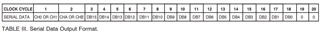
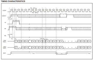
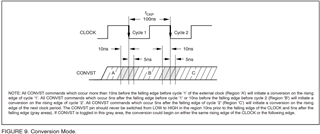
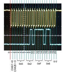
   Getting 16 bit data as o/p from ADC instead of 20 bit , given the 20 sclks for reading the values from SPI.

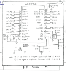
mode pins  M0 = 0 , M1 = 1, A0 =0

reference  = internal reference 2.5 v

SPI in receive only mode with 10mhz frequency.

i/p voltage                  value

 1.2744 v                   0x8280

1.0021 v                   0x65c0

0.5079 v                   0x3464

  • Hello Priti, 

    Could you please share a screenshot either form a logic analyzer or an oscilloscope of the digital pins during the data transfer? If possible a schematic as well? 

    The ADS8361 is a 16-bit ADC, so the data output should be 16-bit. The data transfer should be in a 20-bit format meaning that it requires the 20 clocks, the 1st bit represents the mux channel number (with M0 = 0, M1= 1, A0= 0, this would be Ch 0 making this bit logic low), then the ADC channel (toggling between ChA & ChB), then the 16-bit ADC data, and lastly 2 bits set to 0. 


    Best regards, 

    Yolanda

  • Hello Priti, 

    From what I can tell there in your scope it looks like the data was CHA0: 0x1BE4 which should be roughly 544mV does that correlate with the input on CHA0?

    Could you please share another oscilloscope shot with the CONVST signal included? there is a possibility that the timing is off and the device is getting 19 clocks instead of the 20.  Depending on CONVST the data might be shifted 1 bit and the value might be ~270mV?

    I also noticed that the clock is configured with a CPOL set to 1 (clock polarity is set to high when idle) what is the clock phase set to in your controller? 

    On SDO the data bit transitions on the rising edge of the SCLK and should be read on the falling edge of SCLK. Could you please confirm what protocol is being followed by your controller? and make sure the data is being captured at the falling edges of the SCLK?

    Another important thing to note is the 1st falling edge, this coupled by the CONVST is what initiates the conversion and sets what cycle the data will be valid at.  Depending on the rising edge of CONVST in relation to the falling edge of the SCLK, the data on SDO will start on transitioning on the either the next rising SCLK edge or the one after that (Figure 9 explains this closer).  Would you be able to test this timing? This could help ensure the device is getting the full 20 clocks too. 

    If you measure CH1 of either or both CHA/B the 1st bit should be 1 and could help identify where the beginning of the valid data is set.  

    Best regards, 

    Yolanda 

  •      I have configured clock with CPOL set to high.

    FOR CHA1: input voltage -> 1.0003 V

    CONVST and SCLK

    CONVST and DOUT

    SCLK and Dout

  • Hello Priti, 

    Thank you for sharing those screenshots. 

    Was the last image (SCLK and DOUT) with a different input voltage (not the 1V mentioned at the top)? The DOUT on that picture looks very different than the one on the CONVST and DOUT image.  

    What does the input of the ADC look like?

    I see a "_N" and "_P" with all of your inputs so it looks differential, what is the common mode of your input signals?

    If you are using CPOL = 1, i would recommend you set your CPHA to 0 so the controller reads the valid SDO data on the falling edges, and ignore the 1st falling edge. 

    Below is how I tried to decode the data on your SCLK and DOUT scope shot, 0x02F6 looks more like ~50mV above the common mode of your signal (or ~2.55V if common mode = 2.5V).  

    I tried decoding the CONVST and DOUT as well, but since the other two oscilloscope shots are with 5us/div, and that one is 10us/div it is difficult to confirm. Could you share something similar with both having the same input and same time/div on the oscilloscope? 

    Best regards, 

    Yolanda