Other Parts Discussed in Thread: MSP430F2619, ADS1259
Tool/software:
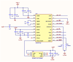
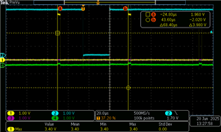
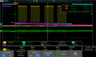
I'm currently working on a tool that includes an ADS1259-q1 and msp430f2619 MCU. Currently, my hardware and firmware are able to read valid data with Chip select (CS) always low (set with GPIO pin), as seen below:
* START = yellow (circled), DRDY = purple, CS = blue, DOUT = green.
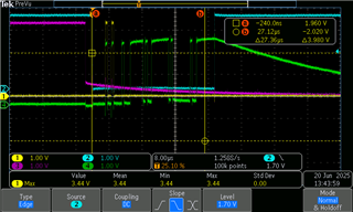
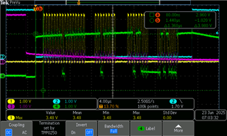
I am preparing for a future design in which 2x ADS1259-q1 will be on one SPI line (sharing SCLK, DOUT, DIN with separate CS, RST, START, DRDY). I am testing a communication scheme that engages the CS with one ADS1259 on one SPI line in preparation. However, when engaging the CS, my DOUT remains inactive. This is shown below:
* START = yellow (circled), DRDY = purple, CS = blue, DOUT = green.
Some notes:
- This is the same hardware that gave me valid results with CS kept low.
- The only difference in firmware between version is whether CS is kept low for entire operation (the working version in first screenshot) or if CS is only brought low for read/write operations (the second screenshot).
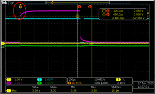
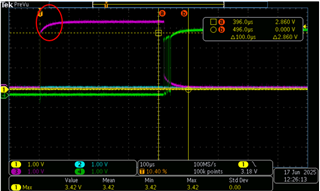
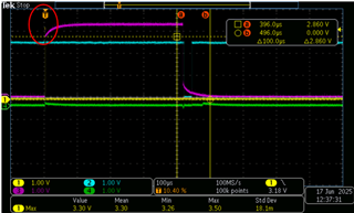
- The datasheet mentions a minimum time between CS low and SCLK rising edge of 50ns. I measure 300ns in my system and have tested with delays up to 15us with no change in behavior.
- Checked pins on ADS1259 and MSP430 side to confirm signals going through.
- MCU uses 16MHz external clock, The ADS SCLK uses SPI clock set to 2 MHz
- ADS1259 register settings (applies to both cases):
- CONFIG0 = 0x05: SPI timeout enabled, Internal reference bias
- CONFIG1 = 0xc0: checksum, out-of-range flag enabled (used to confirm valid data)
- CONFIG2 = 0x17: Pulse Control Mode, 14400sps.
- Offset: not set
- Set to RDATAC
I am looking for additional debug tips to look into as I try to get this working with CS. Also, I would appreciate any advice to consider when designing a system with 2x ADS1259-q1 on one SPI line