This thread has been locked.

If you have a related question, please click the "Ask a related question" button in the top right corner. The newly created question will be automatically linked to this question.

ADS7142-Q1: Clarification on Application note.

Part Number: ADS7142-Q1
Other Parts Discussed in Thread: ADS7142

Tool/software:

Dear Team TI, I was looking forward to implement ADS7142QDQCRQ1 ADC in my design. I was going through the application note of  ADS7142 series ADC and  I got few doubts. Can you please clarify the below.

1. In order to calculate Fsamp(max)( which is fs = oscillator frequency/ nclk from data sheet), If tHSO =110ns, then I will end up getting the oscillator frequency of 9.09 MHz. Now if I use High speed oscillator and if nclk is 21 then, fs = 432.9kHZ. Now this violates the maximum sampling speed of the ADC which is 140Ksps. In this case what will be sampling speed fs of the device?

2. Under component selection, point 4 in Application note, I could see that the target sampling frequency is 10KHZ with the max conversion time 1.8 μs. Is this 10kHz the sampling rate which is assumed and to be incorporated in the design.

3. In ordered to get 10kHz as fs, what should I consider oscillator frequency and nclk?

3. In the calculator shown below,

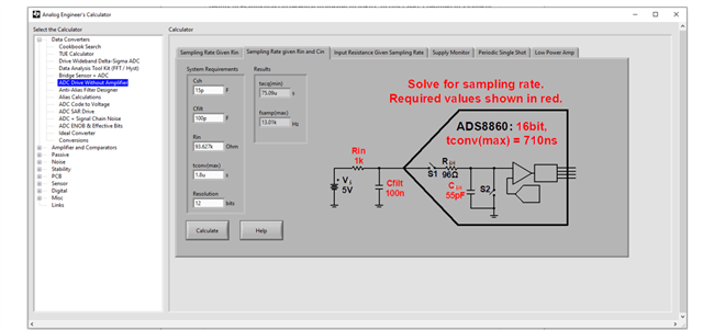
The Rin, Cfilt is not matching with the entered values in the calculator and the values shown in the schematic.

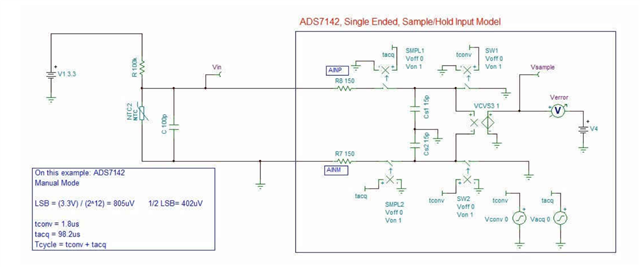
4. Why is Rin not used in the below schematic diagram during simulation? and even though without considered Rin (which was considered for calculating fs based on Cfilt adjustment to get to the nearest value of fs= 10KHz) , C=100pF is considered for the circuit?

Please clarify the above ASAP.

Best Regards,

Srujan L

  • HI Srujan,

    1. The 140kSPS quoted max is considering the maximum speed of the I2C interface, which has limitations given it has some overhead like in address selection, and is half duplex, and not full duplex. Internally, the device can convert at a minimum cycle time of 1us, and set the registers and ALERT pin accordingly, so sampling will essentially be faster in autonomous modes, but you will not be streaming data over the interface in real time.

    2. For this one, can you help share which document and section this is coming from? I wasn't able to find exactly where this was mentioned.

    3. I believe here you are referring to the fact that the input values don't graphically change what is displayed on screen. That is expected. The only parameters that do change are the Results boxes, tacq(min) and fsamp(max).

    4. Rin in the simulation is the equivalent resistance of the pull-up resistor to 3.3V and the NTC thermistor in parallel. Typically, the voltage at the output of a temperature sensing circuit stays relatively stable. The filter capacitor in this case serves to filter higher frequency noise from the input to the ADC, and to help replenish charge to the ADC sampling capacitor. 

    Regards,
    Joel

  •  Dear Joel,

    points 2,3 & 4, I was referring to this document. Monitoring NTC Thermistor Circuit With Single-Ended ADC.

    for point 3, I was saying that in page 3 of  Monitoring NTC Thermistor Circuit With Single-Ended ADC document, The entered input values to the calculator don't match with the component values in the schematic shown in the calculator.

    Best Regards,

    Srujan L

  • Hi Srujan,

    Thanks for clarifying. It seems like the Csh of 15pF is modelled, as well as the Cfilt of 100pF, as is the Rin as a result of R1 || Rntc. Let me know if I missed something.

    Regards,
    Joel