This thread has been locked.

If you have a related question, please click the "Ask a related question" button in the top right corner. The newly created question will be automatically linked to this question.

ADS8665: Getting samples at fixed period without needing to synchronize CS and CLK signals

Part Number: ADS8665


Tool/software:

Hello!

I am using STM32 device to read data from ADS8665 at 48KHz sample rate for audio application. Unfortunately, STM32 SPI hardware does not provide a functionalty for SPI to get samples at a fixed period. Even though it does, i have to toggle CS pin at 48KHz somehow without CPU intervention. I was using software timer interrupts to generate required CS signal and start a SPI DMA transfer, which involves CPU, leading to inconsistent time period between samples. I solved this recently using 2 different timers.

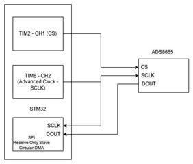
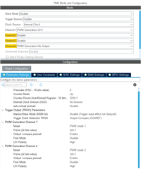
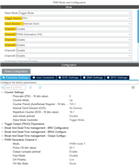
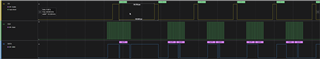
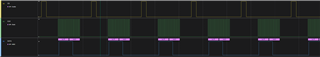
One timer generates CS signal as 48KHz PWM with %20 duty cycle. Other timer works in Trigger mode and when CS timer triggers, this timer generates 16 clock pulses. I used STM32 SPI as slave. Connection is like this:
TIM CLK Signal: Connected to both ADC CLK and STM32 SPI SLAVE CKL

TIM CS Signal: Connected to only ADC CS

ADC SDO: Connected so STM32 SPI SDI

ADC SDI: Low all times

This way, i trick the STM32 as if some master sending data to it, and adc as if master requests data from it. This works but I need an advanced timer of STM32 to provide exactly 16-32 clocks, which can be utilized for more complicated tasks if ADC already handles that itself.

I realized that ADS8665 is capable of providing timer clock from RVS pin, but I have a hard time of this operation of the ADC. If i use it's internal clock, clock output from RVS pin will be very high for my sample rate needs, and this internal clock is not dividable. I wonder if i can provide an external

48KHz continous CS signal with 50% duty cycle

2MHz continuous CLK signal with 50% duty cycle

and ADC outputs samples from SDO, also providing 32 bit clock signal from RVS, so that I can still use STM32 SPI in circular DMA mode by connecting RVS to STM SPI CLK and ADC SDO to STM SDI?

If not possible, is there any way to get ADC samples without CPU intervention?

Thanks in advance!

  • Hi Cagri,

    Welcome to our e2e forum!  What you are proposing does sound like a viable option for the use of the ADS8665.  I'm not aware of anyone trying this before so please do let me know how it works out.

  • Sure! I will share how I received fixed sample rate using stm32 hardware timers. But as I said, it would be great if I can somehow give this job to ADS8665. Current spi output clock frequency over RVS pin is very high. It would be awesome if there's any way to reduce it and also keep the data and clock in sync. 

  • Hi Cagri,

    When you apply the external 2 MHz clock to SCLK, that will be the RVS clock output - review section 7.5.4.2.3.1 in the datasheet (page 46).

  • Hello!

    If you're interested, I found a way to achieve a periodic sampling rate from the ADS8665 ADC using STM32 configured as an SPI slave, all without any CPU involvement. In this setup, although STM32 is not the SPI master, it essentially controls the timing signals—mimicking master behavior to bit-bang data from the ADC. Here's how I connected everything:

    I'm using TIM2 to generate the Chip Select (CS) signal for the ADS8665. TIM2 not only controls the CS line but also acts as a trigger source for TIM8, which is responsible for generating the SPI clock. Each time the CS line is toggled, the ADS8665 captures a sample from its analog input. Shortly after CS goes active, TIM8 is triggered to output a 50% duty cycle PWM with 16 pulses, which serves as the SPI clock signal. Below is how it's configured in STM32CubeIDE:

    Both timers run at 108 MHz, and by dividing this frequency by 2250, I achieve the desired 48 kHz sampling rate. In TIM2, Channel 1 is configured to generate the CS signal after 225 timer counts. Channel 4, while not connected to any physical output, is used internally to trigger TIM8. Its compare value is set to 725 to ensure that the clock signal generated by TIM8 is center-aligned with the active CS state. The output trigger source is configured as OC4REF.

    TIM8 is configured in slave mode, with its trigger source set to ITR1, which links it to TIM2. Note that trigger mappings like ITR1 can vary between STM32 models, so it's important to consult the reference manual to verify which timer connects to which ITR input. TIM8 is set to One Pulse Mode and configured with a repetition counter of 16, so it generates exactly 16 clock pulses per trigger. The clock signal is output on Channel 2 at 864 kHz. For a 50% duty cycle, I set the PWM pulse width to 62, which is half of the period value (125).

    On the SPI side, I configured the peripheral in Receive-Only Slave mode with a 16-bit data size. I enabled DMA and NVIC interrupts, and set up the DMA in circular mode with a half-full threshold and half-word (16-bit) data width.

    There are a few important points to handle correctly in code.

    1- You must initialize the slave timer (TIM8) before the master timer (TIM2) in main.c. This ensures proper synchronization and prevents premature triggering.

    int main(void)
    {
    
      /* MPU Configuration--------------------------------------------------------*/
      MPU_Config();
    
      /* MCU Configuration--------------------------------------------------------*/
    
      /* Reset of all peripherals, Initializes the Flash interface and the Systick. */
      HAL_Init();
    
      /* Configure the system clock */
      SystemClock_Config();
    
      /* USER CODE BEGIN SysInit */
      MX_TIM8_Init();
      MX_TIM2_Init();
      /* USER CODE END SysInit */
      
      //rest of the initialization.....
    }

    2- The DMA buffer used for SPI data reception must be properly memory-aligned. If it's not aligned, the data may be misaligned by 1 byte, which can cause incorrect reads and even buffer overflows.

    // This may not work
    struct {
    	volatile uint8_t a;
    	volatile uint8_t b;
    
    	uint8_t raw_buf[K * 2];
    } data_str;
    
    // This does work
    struct {
    	volatile uint8_t a;
    	volatile uint8_t b;
    
    	uint8_t raw_buf[K * 2] __ALIGNED(4);
    } data_str;

    3-To ensure a reliable startup, the initialization sequence is important. You should first start SPI DMA reception, then start the slave timer (TIM8), and finally start the master timer (TIM2). This order guarantees that all components are ready before signals begin to flow.

    void addaq_data_init() {
    	HAL_SPI_Receive_DMA(&hspi2, data_str.raw_buf, BUF_SIZ_BYTES * 2);
    	osDelay(1);
    	HAL_TIM_PWM_Start(&htim8, TIM_CHANNEL_2);
    	HAL_TIM_PWM_Start(&htim2, TIM_CHANNEL_1);
    }

    With everything set up correctly, the system works flawlessly—as confirmed by the waveform captured on the logic analyzer.

    If you notice that the first clock pulse appears too early, it's because TIM2 (the master) was started before TIM8 (the slave). Simply reversing the initialization order—starting TIM8 before TIM2—resolves this issue.

    After making that adjustment, I received the expected ADC value of 0x7FE0 (which corresponds to 0x7FE = 2046), confirming that the data is being correctly written into the raw DMA buffer.

  • Cool!

    Thank you for letting us know!