This thread has been locked.

If you have a related question, please click the "Ask a related question" button in the top right corner. The newly created question will be automatically linked to this question.

TLA2518: TLA2518 returns 0xFFF in OTF mode and 0x00 from register read – possible config issue?

Part Number: TLA2518

Tool/software:

Hi all,
This is my first post in this forum. 

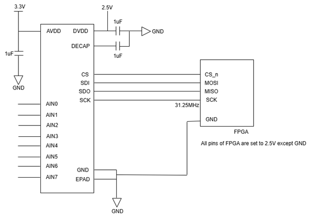
Attached is my circuit schematic. The SPI clock (SCLK) runs at 31.25 MHz, derived from a 125 MHz source clock. I am debugging the design with Signal Tap Logic Analyzer, sampling at 125 MHz to capture the received data; the screenshots are included.

Test sequence

  1. Enable on-the-fly mode by sending the 32-bit command 0x08_10_02_00 from the FPGA to the ADC.

  2. Read channel 2 by sending the frame {2'b10, chan, 7'b0}.

Regardless of the number of attempts, the ADC always returns 0xFFF. I’m trying to determine whether the device is faulty or whether I have missed something in the configuration.

As a cross-check, I connected the same ADC to an ESP32 and tried to read register 0 (SYSTEM_STATUS). It returns 0x00 instead of the expected 0x80 / 0x81.

Could you suggest a systematic way to confirm whether the TLA2518 is working correctly? My ESP32 test code is attached for reference.

Thank you for your help.

  • Hi Sameer,

    Apologies for the delayed response here.

    Instead of a 32-bit command, are you able to send just a 24-bit command?

    From the captures, I'm not exact on what signal corresponds to which digital pin on the ADC. Can you clarify which corresponds to ~CS, SCLK, SDI, and SDO? The issue is likely that the command is not being sent correctly, especially since the SYSTEM_STATUS read is not working.

    Regards,
    Joel

  • Hi Joel,

    Thank you for your response.

    Just to clarify, I am sending only a 24-bit command to the TLA2518. The last 8 bits in the 32-clock burst are padding and not part of the actual command.

    Attached is a Signal Tap capture showing the MOSI (SDI) signal where I sent the command:
    0x08_10_02
    This corresponds to a write command (0x08) to register address 0x10, with data byte 0x02.

    After the 24th clock cycle, the chip-select (~CS / SS_n) is driven high, ending the SPI frame cleanly.

    Please confirm whether this behavior is correct and whether the TLA2518 will reliably latch the command in this setup. If needed, I can remove the 8 padding clocks entirely and ensure ~CS is asserted high immediately after clock 24.

    Let me know if the waveform looks valid or if there is anything I should revise in the timing.

    Thanks again for your support.

    Best regards,
    Sameer

  • Hi Sameer,

    Yes, I confirmed that the device's commands only work with 24-bit SPI frames, a frame being defined while ~CS is low. 32-bit transfers while ~CS is low will not work in the default configuration.

    In all honesty, I'm still a little bit confused by what lines the signals are probing, but it seems like you have the correct idea. As a test, I would start by reading the GENERAL_CFG register with the 0x10 00 00 command. The register data should come out on the first byte of the following SPI frame, which can be anywhere from 12 to 24 bits depending if you are giving a register command or not.

    Regards,
    Joel