This thread has been locked.

If you have a related question, please click the "Ask a related question" button in the top right corner. The newly created question will be automatically linked to this question.

ADS131M08: Synchronize ADS131M08 and the other ADC

Part Number: ADS131M08
Other Parts Discussed in Thread: SN74LV163A, SN74AUP2G80,

Tool/software:

Dear Specialists,

My customer is considering ADS131M08 and has a question.

I would be grateful if you could advise.

---

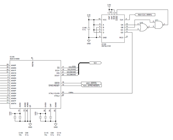
I will be using both the ADS131M08 and the A/D converter built into the microcontroller.

I would like to synchronize the sampling timing of the two devices.

Could you please let me know how to do this?

---

I appreciate your great help in advance.

Best regards,

Shinichi

  • Hi Shinichi,

    The /SYNC pin on ADS131M08 can be used to synchronize conversions between multiple ADS131M08 devices as well as to maintain synchronization with external events. The same clock must be provided to all devices and the SYNC/RESET pins must be strobed simultaneously at least one time to align the sample periods internally between devices. You can check the details in the section 8.5.2 Synchronization and 9.1.5 Multiple Device Configuration in the datasheet.

    -Dale

  • Hi Dale,

    Thank you for your reply.

    I shared your answer with the customer and they have additional questions.

    Could you please advise?

    ---

    ① TI's response and §9.1.5 state that the same clock must be supplied to all devices.

    The MCU's operating clock (48MHz) and the ADS131M08's operating clock (8.192MHz) are different.

    If I divide the microcontroller's operating clock and supply it to the ADS131M08, will it be synchronized?

    ② It says that synchronization is achieved by sending a synchronization pulse from the MCU to the SYNC/RESET pin.

    Is it enough to synchronize once after power is applied? Or should it be synchronized periodically?

    ③ According to §8.5.2, is "synchronization" correct to mean synchronization between the SYNC/RESET pin pulse and the internal clock?

    I don't understand the overall picture of the relationship between the internal clock, CLKIN, and SCLK inside the ADS131M08, and how the internal clock is related to the sampling timing and the digital filter resetting operations. Is there a description somewhere?
    What we ultimately want to synchronize is the sampling timing of the MCU's ADC and the ADS131M08.

    ④ It seems that when a pulse is input to the SYNC/RESET pin, it determines whether it is synchronized with the internal clock, but how much of a discrepancy is necessary to determine synchronization? (I don't think there is a perfect match in timing.)

    ⑤ If the ADS131M08 determines that it is out of sync after sending a pulse to the SYNC/RESET pin from the MCU, is there a way for the MCU to recognize this?

    ---

    I appreciate your great help and cooperation.

    Best regards,

    Shinichi

  • Hi Shinichi,

    Please see the answers below:

    1. Using the same clock source is a basic requirement for synchronization, however at least one time synchronization by sending a pulse to the /SYNC pin should be implemented.

    2. Considering the clock shift and the delay to the ADCs, periodical synchronizations are recommended. 

    3. The internal modulator clock is half of the main clock that is applied to the CLKIN pin, the output data rate = modulator clock/OSR, where the OSR (oversampling radio) represents the ratio of the modulator's sampling rate to the desired output data rate. The digital filter decimates data which is output from the modulator at modulator clock frequency by a factor known as the OSR. I would recommend the customer to watch the videos to learn more: precision labs series: Analog-to-digital converters (ADCs)

    4. It is possible to see a small delay from the clock on your microcontroller to the ADC, but usually it can be neglectful. A negative pulse on the /SYNC pin of ADS131M08 with a duration less than tw(RSL) but greater than a CLKIN period is the right way to trigger a synchronization.

    5. No, it happens shortly.

    BR,

    Dale

  • Hi Dale,

    Thank you for your reply.

    I shared the information with the customer.

    When the customer has an additional question, I'll consult the other post.

    I appreciate your great help and cooperation.

    Best regards,

    Shinichi

  • Hi Shinichi,

    Sounds good.

    BR,

    Dale

  • Hi Dale,

    The customer considered a circuit based on your suggestion, and has additional questions.

    Could you please advise?

    ---Questions

    1. The sampling rate of the A/D converter built into the microcontroller is 1953.125 SPS.
    I believe the same sampling rate can be achieved by setting the ADS131M08's MASTER CLOCK to 8MHz (fMOD=4MHz) and OSR to 2048.
    Is this correct?

    2.
    You mentioned it's recommended to periodically send a pulse from the microcontroller to the SYNC/RESET pin for synchronization.
    Does this mean that the microcontroller sends a pulse to the ADC at the DRDY timing (i.e., at a cycle of 1/1953.125 or an integer multiple of that)?

    (The datasheet mentions in section 8.5.2 Synchronization that "If the negative edge on SYNC/RESET aligns with the internal data rate clock, the device is determined to be synchronized and therefore no action is taken." I'd like to confirm my interpretation of this sentence.)

    3. The microcontroller's built-in ADC operates based on the timing of the internal 48MHz on-chip oscillator.
    We are considering using a circuit (SN74LV163A) that divides this clock by 6 and supplies it to the ADS131M08.
    In this case, there will be a slight delay in the divider circuit, will this delay be considered "synchronized"

    ーーー

    I appreciate your great help and cooperation.

    Best regards,

    Shinichi

  • Hi Shinichi,

    1. Correct, the expected data rate can be achieved with  8MHz clock and 2048 OSR on ADS131M08.

    2. No need to synchronize in every cycle, they can be synchronized for integer multiple of cycles, it really depends on how long or how much mismatching will be seen in the customer's circuit.

    3. This delay will contribute on the mismatching, but it depends on whether this delay or mismatching is acceptable to the customer. SN74AUP2G80 is used on ADS131M08EVM to divide the 8.192MHz to 4.096MHz and 2.048MHz clock for the ADC on the EVM, see the schematic in the user guide, SN74AUP2G80 has tpd = 4.4 ns maximum at 3.3 V (5.5ns at CL=15pF), SN74LV163A has tpd = 15ns maximum at CL=15pF over temperature. Just for your reference. Please notice the synchronization between ADCs was not considered when SN74AUP2G80 was designed on the EVM.

    BR,

    Dale