Part Number: ADS8689
Tool/software:
Hello,
I am currently working on a project using a PIC16F15356 microcontroller and the ADS8689 ADC to read 8-channel 4–20 mA current signals through a MUX, and send the data to a PC via Modbus.
The communication between the MCU and the ADS8689 is implemented using hardware SPI.
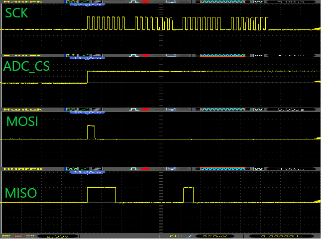
At the moment, when I input 4 mA (approximately 1 V), the raw ADC value is around 25,000. However, even when I try to adjust the input voltage range of the ADS8689 using spi_write, the setting does not seem to take effect at all.
I need the full resolution of the ADS8689 for a 0–5 V input range, but currently I'm unable to configure it properly.
I would really appreciate your advice or suggestions on how to resolve this issue.
Thank you for your help.
main.h
#include <16F15356.h>
#device ADC=10
#use delay(internal=32MHz)   // Use internal oscillator at 32MHz

// -------------------- FUSE Configuration --------------------
#fuses NOWDT           // Disable Watchdog Timer
#fuses NOEXTOSC        // Disable external oscillator
#fuses NOBROWNOUT      // Disable brown-out reset
#fuses SAF             // Enable Storage Area Flash
#fuses PROTECT         // Enable code read protection

// -------------------- UART Configuration --------------------
#pin_select U1TX = PIN_C6     // UART TX pin
#pin_select U1RX = PIN_C7     // UART RX pin
#use rs232(baud=9600, parity=N, xmit=PIN_C6, rcv=PIN_C7, bits=8, stream=PORT1)
// Set up UART1 with 9600 baud, 8N1 format, stream name = PORT1

// -------------------- SPI Configuration --------------------
// Hardware SPI1
#pin_select SCK1 = PIN_C3     // SPI1 Clock pin
#pin_select SDI1 = PIN_C4     // SPI1 MISO pin
#pin_select SDO1 = PIN_C5     // SPI1 MOSI pin
#use spi(MASTER, SPI1, BAUD=500000, MODE=0, BITS=8, STREAM=SPI_1)
// SPI1 hardware setup, mode 0, 500kbps, 8-bit

// -------------------- Type Definitions --------------------
#define uint8     char
#define uint16    unsigned int16
#define uint32    unsigned int32

// -------------------- LED Pin Definitions --------------------
#define LED_RX   PIN_A5   // Red LED (Rx indicator)
#define LED_TX   PIN_A4   // Green LED (Tx indicator)
#define LED3     PIN_A6
#define LED4     PIN_A7
#define LED5     PIN_C0
#define LED6     PIN_C1

// -------------------- ADS8689 Chip Select --------------------
#define ADS8689_CS      PIN_C2   // Chip Select for ADS8689

// -------------------- MUX36S08 Channel Select Pins --------------------
#define MUX_A0  PIN_A0   // MUX select A0
#define MUX_A1  PIN_A1   // MUX select A1
#define MUX_A2  PIN_A2   // MUX select A2

// -------------------- Timer0 Reload Value --------------------
#define TIM0_1ms        (256 - 95)   // Timer0 1ms reload value (based on system clock)

// -------------------- System Time Counter --------------------
uint16 Sys_ms = 0;   // Global millisecond counter (incremented by Timer0 ISR)
main.c
// Called every 1ms by Timer0
#INT_TIMER0
void TIM0_ISR(void)
{
   CLEAR_INTERRUPT(INT_TIMER0);       // Clear Timer0 interrupt flag
   SET_TIMER0(TIM0_1ms);              // Reset Timer0 for next 1ms
   Sys_ms++;                          // System millisecond counter
   UART_Rx.ms++;                      // UART receive delay counter
}

// ---------------- Port Initialization ----------------
// Configure pull-up resistors for each I/O port
void PORT_Init(void)
{
   PORT_A_PULLUPS(0x00);  // Disable pull-up on RA4~RA7 (used for LEDs)
   PORT_B_PULLUPS(0xC3);  // Enable pull-up on RB0, RB1, RB6, RB7
   PORT_C_PULLUPS(0xC4);  // Enable pull-up on RC2 (CS), RC6 (TX), RC7 (RX)
}

// ---------------- MCU Initialization ----------------
// Initialize ports, UART, and timer
void MCU_Init(void)
{
   PORT_Init();                          // I/O pull-up config
   UART_Init();                          // Initialize UART for Modbus

   SETUP_TIMER_0(RTCC_INTERNAL | RTCC_DIV_2 | RTCC_8_BIT);  // 1ms tick setup
   ENABLE_INTERRUPTS(INT_TIMER0);        // Enable Timer0 interrupt
   ENABLE_INTERRUPTS(PERIPH | GLOBAL);   // Enable all interrupts
}

// ---------------- Modbus Request Handler ----------------
// Handle incoming Modbus commands (0x0100, 0x0200, etc.)
void DoCommand()
{
   Modbus_Branch_Process();   // Dispatch based on Modbus address
}


// ---------------- Main Program Entry ----------------
void main()
{
   MCU_Init();                      // Basic MCU peripherals initialization
   ADS8689_Init();                  // Initialize ADC + MUX + SPI + registers
   ADC_Coeff_Init();                // Load calibration coefficients
   modbus_init_slave(1);           // Initialize Modbus RTU slave (ID = 1)

   while (TRUE)
   {
      ADC_Scan();                  // Read ADC values periodically
      DoCommand();                 // Handle Modbus commands
   }
}
ads8689.h
#define CH_MAX             8   // Number of ADC channels

#define COEF_ADC2uA_512V   0.3125   // Conversion factor: ADC → uA (5.120V / 65536 / 250Ω)
#define COEF_uA2ADC_5V     3.2768   // Conversion factor: uA → ADC (65536 / 20000)

#define COEFF_DEFAULT      1.0      // Default calibration gain
#define OFFSET_DEFAULT     0.0      // Default calibration offset

#define ADC_READ_TIME_MS   125      // ADC reading interval per channel (ms)

uint16 ref_buff[2][CH_MAX];     // Reference values for calibration: 4mA, 20mA
uint16 meas_buff[2][CH_MAX];    // Measured ADC values at 4mA, 20mA

uint16 FBuff_mA[CH_MAX];        // Converted current in uA (for Modbus)
uint16 FBuff_ADC[CH_MAX];       // Converted ADC value scaled for 0–5V (for Modbus)

float Coeff_uA[CH_MAX];         // Calibration gain per channel
float Offset_uA[CH_MAX];        // Calibration offset per channel

// -------------------------------------------------------------------------
// Select MUX channel (0~7)
// -------------------------------------------------------------------------
void MUX36S08_Select(uint8 ch)
{
   output_bit(MUX_A0, bit_test(ch, 0));
   output_bit(MUX_A1, bit_test(ch, 1));
   output_bit(MUX_A2, bit_test(ch, 2));
}

// -------------------------------------------------------------------------
// Read ADC value from ADS8689 (32-bit output, upper 16-bit used)
// -------------------------------------------------------------------------
uint16 ADS8689_ReadADC(void)
{
   uint8 i;
   uint8 rx[4];
   uint32 value;

   output_low(ADS8689_CS);

   for(i = 0; i < 4; i++)
      rx[i] = spi_read(0x00);  // Send dummy 0x00 to receive data

   output_high(ADS8689_CS);

   value  = ((uint32)rx[0] << 24);
   value |= ((uint32)rx[1] << 16);
   value |= ((uint32)rx[2] << 8);
   value |= ((uint32)rx[3]);

   return (uint16)(value >> 8);  // Use only upper 16-bit data
}

// -------------------------------------------------------------------------
// Write to ADS8689 internal register (32-bit format)
// -------------------------------------------------------------------------
void ADS8689_WriteRegister(uint8 addr, uint16 write_data)
{
   uint8 tx_buf[4];

   tx_buf[0] = 0xD0 | ((addr & 0x3F) >> 1);  // Command + address MSB
   tx_buf[1] = (addr << 7);                 // Address LSB
   tx_buf[2] = (uint8)(write_data >> 8);    // Data MSB
   tx_buf[3] = (uint8)(write_data & 0xFF);  // Data LSB

   OUTPUT_LOW(ADS8689_CS);
   delay_us(1);

   for (uint8 i = 0; i < 4; i++)
      spi_write(tx_buf[i]);

   delay_us(1);
   OUTPUT_HIGH(ADS8689_CS);
}

// -------------------------------------------------------------------------
// ADS8689 Initialization: MUX, SPI pins, range configuration
// -------------------------------------------------------------------------
void ADS8689_Init(void)
{
   // 1. Initialize MUX select lines
   output_low(MUX_A0);
   output_low(MUX_A1);
   output_low(MUX_A2);

   // 2. Configure SPI pins
   OUTPUT_LOW(PIN_C3);  // CLK
   OUTPUT_LOW(PIN_C5);  // MOSI
   INPUT(PIN_C4);       // MISO
   output_high(ADS8689_CS);  // Deselect ADS8689

   delay_ms(50);  // Wait for power to stabilize

   // 3. Set output format and voltage range
   ADS8689_WriteRegister(0x10, 0x7D08);  // DATAOUT_CTL_REG
   ADS8689_WriteRegister(0x14, 0x000B);  // RANGE_SEL = ±2.5V (5.12V span)

   delay_ms(2);
}

// -------------------------------------------------------------------------
// Convert raw ADC value to uA and scaled ADC (0~5V)
// -------------------------------------------------------------------------
void Convert_ADC_to_mA(uint8 ch, uint16 adc_val)
{
   float uA = 0, val = 0;

   if (adc_val < 8000)  // Consider disconnected input
      uA = 0;
   else {
      val = (float)adc_val * COEF_ADC2uA_512V;
      uA = val * Coeff_uA[ch] + Offset_uA[ch];
   }

   FBuff_mA[ch] = (uint16)uA;

   val = uA * COEF_uA2ADC_5V;
   if (val > 65535) val = 65535;
   FBuff_ADC[ch] = (uint16)val;
}

// -------------------------------------------------------------------------
// Initialize calibration coefficients for each channel
// -------------------------------------------------------------------------
void ADC_Coeff_Init()
{
   uint16 ch;
   uint16 ref0, ref1, meas0, meas1;
   float coeff, offset;

   for(ch = 0; ch < CH_MAX; ch++)
   {
      ref0 = ref_buff[0][ch];
      ref1 = ref_buff[1][ch];
      meas0 = meas_buff[0][ch];
      meas1 = meas_buff[1][ch];

      Coeff_uA[ch] = COEFF_DEFAULT;
      Offset_uA[ch] = OFFSET_DEFAULT;

      if((ref1 > ref0) && (meas1 > meas0))
      {
         coeff = (float)(ref1 - ref0) / (float)(meas1 - meas0);
         offset = (float)ref0 - (float)meas0 * coeff;

         Coeff_uA[ch] = coeff;
         Offset_uA[ch] = offset;
      }
   }
}

// -------------------------------------------------------------------------
// Periodically scan all channels using MUX + ADC
// -------------------------------------------------------------------------
void ADC_Scan(void)
{
   static uint16 prev_ms = 0;
   static uint8 ch = 0;

   if(Sys_ms - prev_ms < 125) return;  // Run every 125ms
   prev_ms = Sys_ms;

   MUX36S08_Select(ch);        // Select current MUX channel

   delay_ms(2);
   ADS8689_ReadADC();          // Dummy read
   delay_ms(2);

   uint16 adc_val = ADS8689_ReadADC();  // Real conversion result
   Convert_ADC_to_mA(ch, adc_val);      // Convert & save

   ch++;
   if (ch >= CH_MAX) ch = 0;  // Next channel

   delay_ms(10);  // Optional delay for settling
}