This thread has been locked.

If you have a related question, please click the "Ask a related question" button in the top right corner. The newly created question will be automatically linked to this question.

ADC12D1600RF: ADC12D1600RF

Part Number: ADC12D1600RF


Tool/software:

Hello,

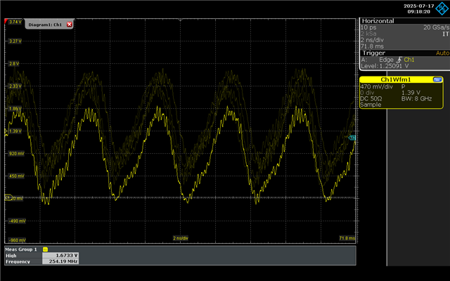
I am expecting the DCLKI output to always have a 50% duty cycle with a frequency of Fs/4 in 1:2 DMUX mode. Can you confirm DCLKI will always have a 50% duty cycle please?

I have a VHDL process that is sensitive to DCLKI and as a test, the process generates a further clock as follows:

p_combine_adc_samples_rising : process(i_DCLKI, reset_n)

variable yy : std_logic := '0';

begin

if rising_edge(i_DCLKI) and reset_n = '1' then


yy := not yy; 
gpio(4) <= not yy;

......

Thank you

  • The sampling clock is 1 GSPS which means DCLKI should have a frequency of Fs/4 = 250 MHz in 1:2 DMUX mod and the above vhdl process should halve this to125MHz, it's the lack of a 50% duty cycle that concerns me, please see the attached waveforms of the 125 MHz output:

    Thank you and kind Regards

  • I have a further update, if I route DLCKI directly to an output, I see the following waveforms which concern me and may explain the above strange duty-cycle behaviour:

    What are your comments?

    Thank you and kind regards.

  • Hi Rajan,

    The output clock should be 1/2 the sample clock.  From the output of the DCLK it looks like your sample clock is dropping a cycle so the DCLK drops a cycle.  Cand you verify your input sample clock is not dropping cycles?

    Regards,

    Geoff

  • Geoff,

    I have checked the 1 GSPS clock entering the ADC and it is perfect in terms of signal integrity and duty cycle as measured and plotted differentially below:

    The ADC is being used in 1:2 DMUX mode which means DCLKI should be Fs/4, i.e. 250 MHz. I have looked at multiple captures on the scope, in Run Stop and Single Stop modes, and the sampling clock is fine!

    Kind Regards,

    Rajan

  • Good Morning Geoff,

    I have modified the VHDL and added an on-command calibration signal prior to digitisation: the resulting DCLK output (250 MHz) which is used to trigger the vhdl processes has also been routed to a GPIO pin and it looks better now:

    However, the FS/8 (125 MHz) output generated with the VHDL processes as a test signal now looks bad, but it's the above clock that is important.

    Comments ....

    Thank you and kind regards

  • added the following to my vhdl and all other processes now require i_cal_complete to be = 1

    p_on_command_calibration : process(i_DCLKI, reset_n)

    -- power-on calibration occurs after a time delay, set by the CalDly pin, following the application of power
    -- when CalDly is low, delay is 2^24 cycles, i.e. 16.7 ms, when CalDly is high, delay is 2^30 clock cycles, i.e. 1.07 s

    -- on-command calibration is iniatated by bringing CAL pin high for a min. of tCAL_H (1280) clock cycles after
    -- it has been low for a min of tCAL_L (1280) clock cycles, 1280 * Ts = 1.28us

    -- CalRun is high during the calibration sequence, otherwise low

    variable tmp : integer := 1;

    begin

    if rising_edge(i_DCLKI) then

    if i_cal_complete = '0' then
    tmp := tmp + 1;
    end if;

    if tmp > 400 then -- 400 DCLKI (FS/4) cycles > 1280 Ts cycles
    adc_cal <= '1';
    elsif tmp > 800 then
    adc_cal <= '0';
    i_cal_complete <= '1';
    end if;
    end if;

    end process p_on_command_calibration;