This thread has been locked.

If you have a related question, please click the "Ask a related question" button in the top right corner. The newly created question will be automatically linked to this question.

TLC2578 not sending output data

Other Parts Discussed in Thread: TLC2578, MSP430F5438, TLC3578

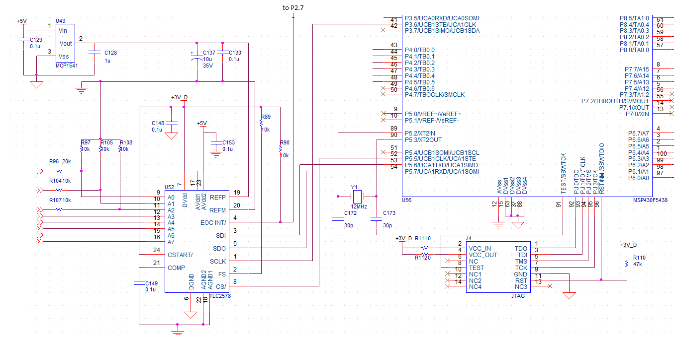
I'm having trouble getting my ADC to respond with an output.  My code pertaining to the ADC is as follows:

P3SEL = 0x70; // P3.4-6 = USCI_A0 TXD,RXD; USCI_A1 CLK
. . . 
P5SEL = 0xEC; // Enable XT2 Ports, Enable USCI_A1 SIMO,SOMI

. . . 
// Clock Setup
	UCSCTL6 &= ~XT2OFF;									// Enable XT2
UCSCTL3 |= SELREF_2; // FLLref = REFO
UCSCTL4 |= SELA_2; // ACLK=REFO,SMCLK=DCO,MCLK=DCO

do // Loop until XT1,XT2 & DCO stabilizes
{
UCSCTL7 &= ~(XT2OFFG + XT1LFOFFG + XT1HFOFFG + DCOFFG);
// Clear XT2,XT1,DCO fault flags
SFRIFG1 &= ~OFIFG; // Clear fault flags
}while (SFRIFG1&OFIFG); // Test oscillator fault flag
UCSCTL6 &= ~XT2DRIVE0; // Decrease XT2 Drive according to expected frequency
UCSCTL4 |= SELS_5 + SELM_5; // SMCLK=MCLK=XT2
. . . 
// TLC2578 Setup
UCA1CTL1 |= UCSWRST; // **Put state machine in reset**
UCA1CTL1 |= UCSSEL_2; // SMCLK
UCA1CTL0 |= UCMSB + UCMST + UCSYNC + UCMODE_2; // Synchronous, Master, MSB First, 4-pin AL
UCA1CTL1 &= ~UCSWRST; // Starts state machine
. . .
// Timer Setup
TA0CCTL0 = CCIE; // Interrupt Mode
TA0CCR0 = 49152-1; // 49152 cycles -> 3 s timer
TA0CCTL1 = CCIE; // Interrupt Mode
TA0CCR1 = 8192-1; // 8192 cycles -> 0.5 s timer
TA0CCTL2 = CCIE; // Interrupt Mode
TA0CCR2 = 12288-1; // 12288 cycles -> 0.75 s timer
TA0CTL = TASSEL_1 + MC_1 + ID_1 + TACLR; // ACLK, up, Input Divider = 2, clear TAR
. . . 
// TLC2578 Init
unsigned char trash;
UCA1TXBUF = 0xAA; // Sends bits 15-8
while(!(UCA1IFG & UCTXIFG))
trash = UCA1RXBUF;
UCA1TXBUF = 0x40; // Sends bits 7-0
while(!(UCA1IFG & UCTXIFG))
trash = UCA1RXBUF;
 . . .
#pragma vector=TIMER0_A0_VECTOR
__interrupt void TIMER0_A0_ISR(void)
{
unsigned char trash;
// TLC2578 Trigger Sequence
UCA1TXBUF = 0x08; // Sends bits 15-8
while(!(UCA1IFG & UCTXIFG))
trash = UCA1RXBUF;
UCA1TXBUF = 0x40; // Sends bits 7-0
while(!(UCA1IFG & UCTXIFG))
trash = UCA1RXBUF;
// Internal ADC Trigger Sequence
ADC12CTL0 |= ADC12SC; // Start internal ADC conversion
}
. . . 
#pragma vector=TIMER0_A1_VECTOR
__interrupt void TIMER0_A1_ISR(void)
{
int data1 = 0;
int data2 = 0;
		UCA1TXBUF = 0xE8;									// Sends bits 15-8, FIFO Read
while(!(UCA1IFG & UCTXIFG))
data1 = UCA1RXBUF; // Store bits 15-8
UCA1TXBUF = 0x00; // Sends bits 7-0
while(!(UCA1IFG & UCTXIFG))
data2 = (UCA1RXBUF & 0xF0); // Store bits 7-4, discard 3-0
V27Supply = (data1*256+data2)/16; // Combine into 12-bit result
*(This is repeated for multiple channels)
}
Any help would be appreciated.


  • Hi Alexander,

    Can you send us a schematic that shows how you have the various control pins of the TLC2578 connected/wired to your MSP430?  If you could send us a screen shot of the MSP430 communication (SCLK, SDI, SDO, EOC/INT, etc) that would be helpful as well. 

  • Hi Tom,  

    here is the section of my schematic involving the TLC2578:

    the microcontroller in use is an MSP430F5438.  As for screenshots, I'm using an older model that does not save screen captures except as .wfm files.  From what I can tell probing at the chip pins with the oscilloscope, the SCLK becomes active during transmission, and the SDI pin sees 3V highs in the correct bit locations.  However, the SDO pin puts out what appears to be noise, and the EOC\INT pin (supposed to be configured as INT) never drops low.  Thanks for your help,

    --Alex--

  • Dear Tom,

    I'm looking over 8686.TLC3578.c as a guideline for interfacing with the 2578, and I was curious why most of the subroutines transmit 4 bytes at a time?  I thought the 2578 and 3578 only needed 2 bytes to send and read data concurrently.  Thanks,

    --Alex--

  • Hi Alex,

    You only need 16 clocks, so 2-byte wide transfers should be sufficient.  What do you get back from the device if you send one of the self test commands?  These are 0xB0, 0xC0 or 0xD0? 

  • The self-test commands seem to work fine,  the data set following each command returned 1/2*Refp, 0, and Refp when sent in order

  • Are you seeing the EOC/INT?  Are the logic levels on SDO consistent with the digital power rail?

  • The levels are running at 3V high which checks out, and the INT* is triggering ~2 us after the end of the Self-test command.  From that information, I presume it must be a problem in the way I'm trying to configure the ADC for the actual channel conversions?

    --Alex--

  • That all sounds right to me.  You have the device configured to use the FIFO (CFR = A40) so after configuration, you essentially write a 'select' command (0x0000 for instance) eight times before the FIFO will trigger.  During these eight select commands, you will not be getting any data out of the SDO.  You might consider trying the single shot mode instead.  This will give you faster overall throughput with the MSP430 I believe and may help you during the initial debug stages.  Try changing your A40 to A00 and see what happens. 

  • So far no effect,  I shifted to a bare bones version of my code to drive only the 2578 (shown below).  This code worked when using self-test commands.  Also, I don't understand the need for 8 select commands to trigger the FIFO.  My understanding of the datasheet was that it needed a configure, a select to initiate the sweep, and then it was a matter of reading the FIFO data.  Is this incorrect?  Also, if so, would a sweep need correct select commands or would they be dummy commands and the sweep would follow the configured order?

    --Alex--

    #include "msp430x54x.h"

    void main(void)
    {
    WDTCTL = WDTPW+WDTHOLD; // Stop watchdog timer
    int trash, trash1, trash2;
    P2IE = 0x80; // Interrupt on P2.7
    P2IES = 0x80; // Falling edge for P2.7
    P3SEL = 0x40; // P3.6 option select
    P5SEL = 0xC0; // P5.6,7 option select
    P5DIR = 0x20; // P5.5 output
    P5OUT |= 0x20;

    UCA1CTL1 |= UCSWRST; // **Put state machine in reset**
    UCA1CTL0 |= UCMST+UCSYNC+UCMSB; // 3-pin, 8-bit SPI master,
    // MSB
    UCA1CTL1 |= UCSSEL_2; // SMCLK
    UCA1MCTL = 0; // No modulation
    UCA1CTL1 &= ~UCSWRST; // **Initialize USCI state machine**

    P5OUT &= 0xDF;
    while (!(UCA1IFG&UCTXIFG)); // USCI_A0 TX buffer ready?
    trash = UCA1RXBUF;
    UCA1TXBUF = 0xA0;
    while (!(UCA1IFG&UCTXIFG)); // USCI_A0 TX buffer ready?
    trash1 = UCA1RXBUF;
    UCA1TXBUF = 0x00;
    while (!(UCA1IFG&UCTXIFG)); // USCI_A0 TX buffer ready?
    trash2 = UCA1RXBUF;
    UCA1TXBUF = 0x00;
    while (!(UCA1IFG&UCTXIFG)); // USCI_A0 TX buffer ready?
    trash1 = UCA1RXBUF;
    UCA1TXBUF = 0x00;
    P5OUT |= 0x20;
    __bis_SR_register(GIE); // CPU off, enable interrupts
    }
  • I figured out my problem with the one-shot code in my last post.  It seems I was not cycling the CS* line, the one shot code works now.  I am still curious about why the sweep mode would need 8 separate select codes?  Thanks for all your help,

    Sincerely,

    --Alex--

  • Hi Alex,

    The TLC2578 has a CSTART pin as well.  If you were to use the CSTART interface to manage the conversion sequence, you would not need to send the 'SELECT' commands.  Take a look over the 'SWEEP Mode' description on page 24 of the TLC2578 data sheet.  When using /CS as the conversion start mechanism, you have to send 'dummy' commands to the device. 

    These dummy commands are the channel select - it does not matter which one you send, they can all be 0x0000 or you can cycle from 0x0000 through 0x7000.  Once the FIFO hits though, you need to send the FIFO READ command eight times to retrieve the data, so basically you are looking at sixteen command/read cycles versus eight in One-Shot mode.  For some of the higher speed processors, this can impact on the efficiency and speed of the overall code, but I'm not so sure that it would buy you anything with the MSP430F5438.