This thread has been locked.

If you have a related question, please click the "Ask a related question" button in the top right corner. The newly created question will be automatically linked to this question.

DAC53204: For eload application problem

Part Number: DAC53204

Tool/software:

Hello,

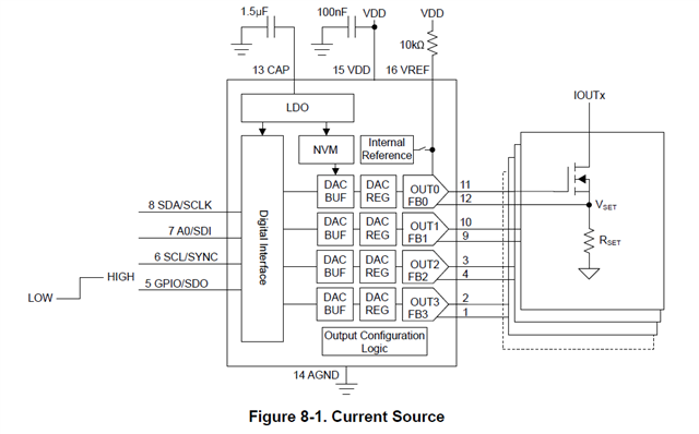
I would like to use below concept to realise eload application from 0~2A.

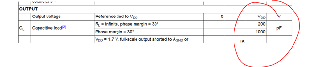
1) in datasheet, there is CL max 200pF.  Does it means external MOSFET gate input capacitance should be small than it?

If yes, please recommend other DAC for me for higher limit. Because most big current MOSFET input capacitance will be about 5~10nF.

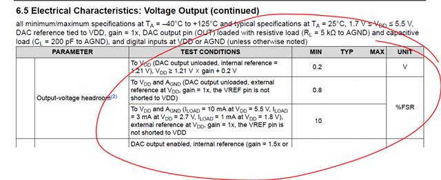
2) For the output headroom, if I don't use external reference, which value should I use? 

The dac53204 VDD is 3.3V and MOSFET gs threshold is 1.2~2.2V and MOSFET drain is connect to VBAT (9V~16V).

Can I achieve full range of 0~2A?  If not, what's the actual range or please recommend other possible DAC part number.

  • Hello, 

    You can add a small series resistance between the DAC output and FET gate if this is a concern. 

    Use the 0.8%FS spec. The output will be unloaded when connecting to a FET. 

    Where is the load in your example if the drain is connected directly to VBAT? 

    Best,

    Katlynne Jones

  • 1) how to choose the small in seriaes reisstor? 

    I suppose 100 ohm should work.

    3.3V/100 ohm = 33 mA < short current limit 50mA.

    Please confirm if it's right.

    2) Where is the load in your example if the drain is connected directly to VBAT? 

    VBAT is from external high side driver outoput. It means MOSFET is the load of high side driver.

    This circuit is used to test high side driver for different current scenario.

    3) For output headroom if using internal reference 1.21V.

    the output up limit should be  1.21-0.2V = 1.01V.

    the output bottom limit should be 1.21*0.8% = 0.009V.

    Please confirm if it's right.

  • Hi Liping, 

    100ohm is fine. The DAC will have reduced performance at 33mA (voltage droop), but the device is operating in closed loop so this should be compensated for. 

    The minimum reference is the internal reference x 1.5x gain setting, so 1.8V. The minimum DAC VDD is also 1.8V. If you are driving output current the headroom requirement becomes higher. For example, the third entry in the headroom table that you shared in the last post is for an output load of 10mA. 

    Best,

    Katlynne jones

  • Could you just give comments just based on my application? It's used to drive MOSFET.

    So, the output range should be go to 0.009V ~1.6V, right?  (as you said 1.8V min, considering 0.2V headrom for top).

  • Hi Liping, 

    There should be no current flowing into the gate of the MOSFET so this is correct.

    Best,

    Katlynne Jones