This thread has been locked.

If you have a related question, please click the "Ask a related question" button in the top right corner. The newly created question will be automatically linked to this question.

ADC108S022: Searching for ADC108S022CIMTX/NOPB replacement options

Part Number: ADC108S022
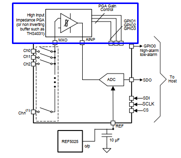
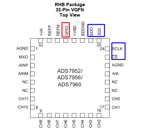
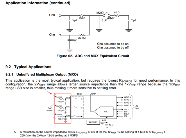
Other Parts Discussed in Thread: THS4031, , ADS7956

Tool/software:

Hi team,

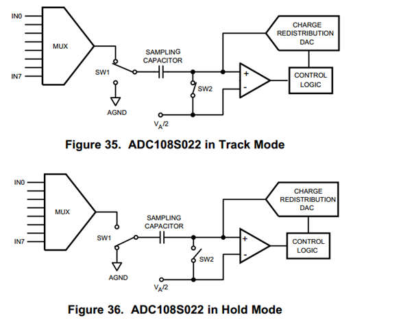
The current project requires an ADC with similar functionality to ADC108S022CIMTX/NOPB but with 10 channels. Are there any recommended ADC models that meet these requirements? Thank you.

Must ensure 10-bit resolution, 10 channels, SPI interface.

  • Hi Sheng,

    The ADS7956SRHBR is a 10-bit, 12-channel, SPI interface. This would be the best recommendation for your requirements.

    -Kyle

  • Hi Kyle R. Stone

    Thank you for your reply.

    I have also looked up information about the ADS7956SRHBR and initially determined that it meets our requirements. However, I still have a few questions that I hope you can help clarify:

    ① What are the specific advantages of adding an external PGA (e.g., THS4031) to the ADS7956SRHBR?
    Originally, we planned to use the ADC108S022, but since the number of channels to be sampled has increased, we are considering either using two ADC108S022s or a single 10-channel ADC.Our goal is to find a replacement with performance comparable to the ADC108S022, just with two additional channels—primarily for cost considerations.Therefore, considering cost factors, the current design will not include a PGA if the ADS7956SRHBR is used. Without the addition of a PGA, how much impact would there be on the sampling performance compared to the ADC108S022?

    ② The ADC108S022 only requires 4 SPI lines to connect to the CPU, while the ADS7956 has both SPI and GPIO. Is this GPIO a necessary control signal, or can it be left unconnected without CPU control?Or are there any other pins besides GPIO and SPI that must be controlled by the CPU?

    ③ Does TI offer a digital temperature sensor similar to the DL18B20? If so, could you please recommend one?

    Given the tight development schedule, I would greatly appreciate your help in confirming the above details. Thank you very much.

  • Hello,

    The performance impact really depends on the type of input signal being sample. If it is a DC signal or very slow signal such as temperature, you can likely go without using an amplifier, and it is not strictly required. If the input signal is a dynamic, AC signal, it is best to use an amplifier to help drive the RC input of the ADC at higher sampling rates. If you are getting good performance with your current design, then you likely won't need a separate amplifier. You might just need some adjustments to the input RC values.

    The GPIOs don't need to be connected. They are optional, but if unused, I recommend tying them to ground. The CS, SCLK, SDI, and SDO pins are the only pins that need to be connected to the controller for data readback and device configuration.

    For temperature sensor recommendation, I recommend reposting this question on the sensors E2E forum so the appropriate team can follow up.

    Regards,
    Joel

  • Hi Kyle R. Stone

    Thank you for your reply.

    I still have a few questions I'd like you to confirm.

    All the signal sources we use are DC voltage sources, such as DC power supplies for substrates and converted DC voltage values from temperature sensors, which are all slow-changing signals.The maximum conversion rate of the ADC we use is up to 200 ksps.

    ① The input side configurations of ADS7956SRHBR and ADC108S022s are different. As shown in the figure, the left side shows ADC108S022s' input with separate track-and-hold modes, while the right side shows ADS7956SRHBR's input without track-and-hold modes. If we replace ADC108S022s with ADS7956SRHBR, do we need to add or reserve additional RC hold circuits on the input side? Our original design simply connects DC voltage (after being divided by kΩ-level resistors) directly to the ADC input pins (CH0~CHn) without any RC hold circuits.

    ② For ADS7956SRHBR, if the power supply is V(+VA)=3.3V、V(+VBD)=3.3V and V(REF)=2.5V, can the ADC(CH0~CHn) accept 3.3V input voltage? Does the input voltage need to be ≤V(REF)?

    ③ Regarding the reference voltage, the datasheet mentions using low-noise bandgap references like REF5025 to drive this pin. Would it be acceptable if I use a 2.5V generated from a DCDC digital power supply (after bead + capacitor filtering) as the reference voltage for the REF pin?

    Thank you very much.

  • Hi Kyle R. Stone

    Could you please help confirm the issue? Thank you.

  • Hello,

    Apologies for the delay on the response.

    It is a good idea to add an input RC filter, even when measuring DC voltages. For more detail, watch the Driving SAR ADC without amplifiers TI Precision Labs video. It also gives good advice to the selection of input RC values.

    On the ADS7956, Vref sets the full-scale input range of the device. If Vref = 2.5V, you can detect voltages up to 2.5V. In your case, with a 3.3V analog supply, you can supply up to 3.3V to the inputs without damaging the device, but the maximum measured voltage would only be 2.5V. Hopefully that makes sense, but let me know if I can clarify.

    Generally, I would avoid switching regulators for providing the reference voltage of an ADC. Often, the switching/ripple frequency couples as noise to the ADC input, and greatly contributes to gain errors. Linear, low noise power supplies are highly preferred.

    Regards,
    Joel

  • HI.Joel Meraz

    Thank you for your reply. This is very helpful to me.

    ① I compared some parameters of ADC108S022CIMTX/NOPB and ADS7956SRHBR, such as INL, DNL, offset error, SINAD, SNR, THD, and SFDR. The parameters of ADS7956SRHBR are still slightly inferior to those of ADC108S022CIMTX/NOPB. Could you please explain the reasons for these differences?

    ② Are there any specific documents that introduce the impact of parameters such as INL, DNL, offset error, SINAD, SNR, THD, and SFDR on ADC performance?

  • Hello,

    1. These are inherent errors to the design of the ADC, and corresponding performance specifications.. 

    2. These DC and AC specifications are covered in the following videos:
        ADC DC specifications: INL, DNL, Cin, leakage, Vref
        AC & DC specifications: Offset error, gain error, CMRR, PSRR, SNR and THD

    Regards,
    Joel

  • HI.Joel Meraz

    Thank you for your reply. This is very helpful to me.

    ①Regarding the 100kΩ reference input resistor mentioned in the datasheet, what is its purpose? Should it be connected in series with the reference input pin in the circuit design?


  • Hello,

    The 100kΩ reference input resistance is the equivalent load is present to the source driving the reference pin. In essence, the reference input is not a high-impedance input, it draws current during ADC conversions.

    The reference source must be able to drive that load without a significant voltage drop. At Vref = 2.5V, and Rref = 100kΩ, an average of 25uA needs to be supplied. Because of this, it is also important to use decoupling capacitors near the reference input to supply current quickly during spikes.

    Regards,
    Joel