Other Parts Discussed in Thread: LMK04832, LMK04832EVM,
Tool/software:
Dear TI,
I am going to use LMK04832 to provide 65 MHz LVPECL clock signals via AC-coupling to 7 (seven) ADC3683 chips, all placed on a single PCB. The application is “a phase meter” where a low intrinsic phase noise is the critical requirement.
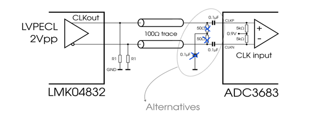
Please consider the following drawing:
I would have these rather subtle questions:
.:1) LVPECL driver DC path and R1 value:
According to SLLA112, R1 shall be in range from 140 to 220 ohm. According to SNAU215A, the value used on LMK04832EVM are 120 and 240 ohm (on some channels there are 120 ohm and on other channels 240 ohm resistors). Since I want to achieve high SNR/SFDR during AD conversion, according to ADC3683 datasheet SBAS872B and its figure 8-14, the higher clock amplitude is beneficial. As such, I am inclined to choose smaller value of R1 to increase current and hence also the differential voltage seen by the clock input of ADC3683. Thus, I would select R1 to be 120 ohm. Would you agree? Or is 240 ohm better choice from some point of view?
.: 2) Termination of the differential clock path at the side of ADC3683
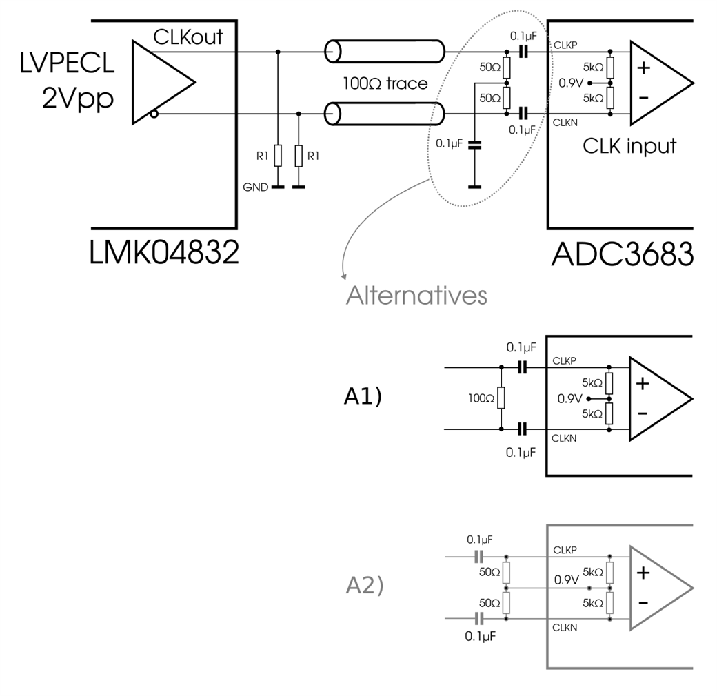
The termination at the end of the transmission line shown at the top part of the picture above is taken from schematic of ADC3683 eval board (DC134-004-REVE_SCH.pdf, available as “ADC3683EVM Design Files” on TI website). I am wondering whether the shown alternatives A1) and A2) could be also considered. A1) seems to be a reasonable option regarding the lower number of used components and according to SLLA112 (if I am interpreting it correctly), this option is good for situation when there is no differential-skew and common-mode noise. It probably does not fully hold in practice, even when all the componnts are placed on a single PCB. A2) is motivated by the availability of the common mode voltage output pin of ADC3683; however, it is probably a bad idea as it changes an operating point within ADC3683 significantly (by adding 50 ohm to 5 kohm in parallel). As such I would stick with the original solution (the top part of the figure above) and would not use the alternatives A1) nor A2). Would you agree?
.: 3 CML instead of LVPECL?
Would there be any benefit of using CML instead of LVPECL for sampling clock at 65 MHz? I understand that for higher frequencies (such above 1 GHz), CML might provide better phase noise (LMK04832 datasheet SNAS688C says that “best performance is achieved with CML in bypass mode”). Am I correct that for such low sampling frequencies the difference between these two standards in terms of phase noise might be negligible? Also, I would prefer LVPECL as it seems it uses lower driving current that CML, hence probably producing smalle self-interferences. Are these thoughts somehow reasonable?
Thank you very much!
Ondrej