Other Parts Discussed in Thread: DAC8775
Tool/software:
Dear Technical Support Team,
Q1
Regarding analog power supply voltage.
When the analog power supply is a single 15V supply and using 0-5V/0-10V/4-20mA , can it output near 0V without any problems?
Does the AVSS listed in the power supply footroom have to be set to -0.5V or less?
Q2
Regarding ESD tolerance, it says ±1.5kV for HBM Is this the performance of the component alone without any protective components?
Or does it mean the tolerance when a circuit like that listed in 9.2 of the data sheet is assembled?
Q3
The various specs in the datasheet are specified under the condition that Vref and DVDD are supplied externally, but how do the specs change when internally generated Vref and DVDD are used?
Information on TUE would be appreciated.
Q4
Regarding the description of short-circuit current, there is a description of typ value in the electrical characteristics, but what is the worst value (min,max) at Ta=25℃?
Q5
There is also a description of short-circuit current for REFOUT and DVDD, but do you have the temperature characteristics for these as well?
Q6
What is the output impedance when Vout is unused?
Q7
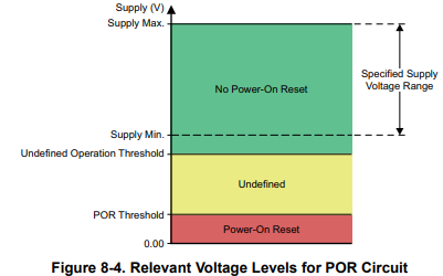
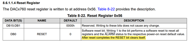
8.3.7 Power-on reset, is there a description of resetting when the reset detection voltage falls below the reset detection voltage for more than 1ms?
How long does it take for the reset to be canceled after the reset voltage is reached?
Q7
I could not find any description of allowable load resistance of current output, but is it correct to think that the limit value of the condition to meet the compliance voltage is the allowable load resistance?
Q8
Do you have any information on the leakage current from Iout when Iout is not used?
Q9
Do you have any information on the accuracy and temperature characteristics of the internally generated DVDD = 4.6V?
Q10
I know from table 7.5 in the datasheet that the current consumption AIDD increases by about 1mA when using the internal DVDD, but how much does it increase when using the internal Vref?
Best Regards,
ttd