ADC3444: Phase Inconsistency Between ADC3444 Chips After Power Cycling

Part Number: ADC3444

Tool/software:

Hello,

We are working with a custom board that integrates multiple ADC3444 chips. These ADCs are grouped such that half of the chips receive their sampling clock from one HMC7044 clock generator, while the other half are connected to a second HMC7044. Both HMC7044 devices receive a common reference clock input, ensuring their outputs are derived from the same frequency reference.

The ADC3444 chips operate at a sampling rate of 122.88 MHz, and this sampling clock is directly generated by the HMC7044s without using any internal dividers in the ADCs.

We’ve observed that the phase relationship between channels across the ADCs is not preserved across power cycles.

Could this behavior be caused by clock input alignment issues to the ADC3444s? Is there a recommended approach for achieving deterministic multi-chip synchronization in such a setup? We understand that SYSREF may not apply here, as no internal clock dividers are used within the ADCs.

Best regards

  • Hi,

    I would investigate to make sure all the HMC outputs to all of the ADC3444s are in phase alignment when they arrive to the ADC's clock pins on startup?

    Has this been verified?

    Regards,

    Rob

  • Hello,

    We are currently examining the phase of the clock being supplied to all inputs. At the moment, we observe that the clock input phase varies across power cycles. Could this variation be the root cause of the issue we're facing?

    Additionally, if the clock inputs are kept in phase, will the ADC outputs also remain phase-aligned? In our current setup, is it possible to achieve output phase alignment using SYSREF or any other method?

    Best regards

  • Hello,

    As mentioned earlier, we are using two HMC7044 chips to provide clock signals to four devices each. We are utilizing the SYNC mechanism in the HMC7044 to synchronize the outputs of both clock chips.

    We have verified the status by reading back the relevant HMC7044 registers and confirmed that both PLL1 and PLL2 are locked. Additionally, the output phases are stable on both devices. When measured on an oscilloscope:

    • The clock signals going to devices from the same HMC7044 are perfectly aligned.

    • The clock signals between the two HMC7044 chips show a small phase difference (typically less than 10 degrees).

    However, despite the clocks from the same HMC7044 being well aligned, we have observed that the ADCs receiving clocks from the same HMC7044 do not always maintain phase alignment between them after power-up. This inconsistency occurs in some power cycles.

    We are seeking guidance on how to debug this phase mismatch issue when using multiple HMC7044 chips. Specifically:

    • Should we expect perfect phase alignment across multiple ADCs when they are clocked by the same HMC7044?

    • Could there be any additional configuration, SYNC timing, or reset sequencing requirements that we might be missing?

    If any further information is needed from our side, we are happy to provide it.

    Best regards

  • Hi,

    The ADC itself does not have a way of synchronizing itself using sysref. After reading the datasheet, the sysref in put is used to synchronize the divided down clock in the ADC to an external sysref edge. So this will not help you in this case as the dividers are not being used. 

    Are you seeing random phases across power cycles or is it always consistently off?

    If it is off consistently, then it could be due to input trace matching? Can you please verify?

    Ideally to test, try to configure the clocking system and power cycle only the ADCs and verify phase consistency here.

    If this fixes the issue, then it is something to do with the clocks because the ADC is not doing anything special with the clocks that could cause random phase power cycle to power cycle.

    Regards,

    Rob

  • Hello,

    In our case, the ADC output phases are random from one power cycle to another. Within the same power cycle, the phases remain constant, but after a power cycle, the phases vary.

    We do not believe this is due to input trace delays, as we observe that all four channels of the same chip maintain almost identical phases. The issue appears to be phase inconsistency between different ADC chips, even though the input clocks are synchronized.

    Could you please confirm—if the clocks are synchronized, should multiple ADC3444 chips always produce constant phase outputs?

    For clarification, our PCB team has confirmed that all data and clock trace lengths are matched for all chips.

    Best regards

  • Hi,

    Please give me a few days, I am working on this with design to see if there is anything I can uncover here.

    Thank you for all the details.

    Regards,

    Rob

  • Hi,

    I spoke with design. Its not clear to me in the previous posts above, but you need to use the SYSREF (SYNC) signal to make sure that the all the internal dividers are synchronized.

    Could you tell us which mode you are putting the ADC in?

    Lastly, if you have a block diagram or schematic to share that would helpful.

    Regards,

    Rob

  • Hello,

    From my understanding and from our previous discussion, SYSREF is only required when internal clock dividers are used. Since I am not using any dividers, I would like to clarify what exactly these internal dividers are.

    In my case, the ADC receives a 122.88 MHz clock, which is also the sampling rate, so no dividers are involved.

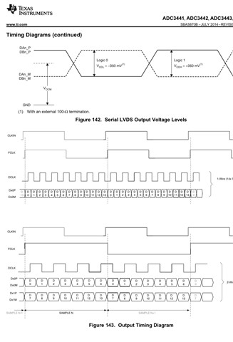
    Regarding the mode, I believe the question is in the context of data transfer from the ADC. I am using a 2-wire interface with 7× serialization, and the data is transmitted at a DDR rate.

    Best regards

  • Hi,

    Thank you for the details. I will get clarity if the dividers still need to be set even if you are not using them.

    I will circle back tomorrow with an update.

    Regards,

    Rob

  • Hello ,

    any update on this ?

    Best regards

  • Hi,

    Let me ping design again. Thanks for your patience.

    Regards,

    Rob

  • Hi,

    Design came back, here are their comments:

    If using 7x serialization, the Frame Clock is at  fs/2 - which means it would require an external sysref to synchronize across chips.

    Can we get more information on the amount of phase slip seen?

    Are the FCLKs coming arbitrarily in and out of phase? 

    Regards,

    Rob

  • Hello,

    We are using 7x serialization and I’d like to share some details about our deserialization approach.

    We are not using the frame clock for deserialization. Instead, we rely on custom patterns from the ADC. The reason for avoiding the frame clock is that we observe skew between the data samples and the frame clock, and this skew is not consistent across power cycles. In some power-ups, the skew is positive, while in others it is negative.

    In TI’s document “Understanding Serial LVDS Capture in High-Speed ADCs”, it is mentioned that skew between the frame clock and the serial data can occur. The document also suggests using a custom pattern embedded in the data, which resembles the frame clock, and then using this pattern for latching the samples at the correct position. In our case, the custom pattern itself serves this purpose.

    Our deserialization logic flow is as follows:

    • Serial data from ADC wires

    • Bit eye scan logic to capture data at the center of the bit window

    • 14-bit gearbox logic

    • Custom pattern used for sample boundary alignment

    • Validation of samples using ramp test pattern

    • Final samples for use

    Given this setup, are we missing something that could be causing the phase misalignment issue?

    Our concern is that the frame clock itself is not aligned with the data, which leads to incorrect bit latching. Even if we used the frame clock for deserialization, we would still need the custom patterns to compensate for the skew. I also want to add that there is skew between the 2 wires of serial data . so we are using test patterens to get sample from correct position from both wires .

    • Can you confirm whether using SYSREF guarantees that there will be no skew between the frame clock and the serial data and also between 2 wires of serial data?

    • Is there anything incorrect in the process I am following that could be causing the phase variation?

    Best regards

  • Hi,

    Thank you for your patience, I spoke to design and here are the following comments:

    “The document also suggests using a custom pattern embedded in the data, which resembles the frame clock, and then using this pattern for latching the samples at the correct position. In our case, the custom pattern itself serves this purpose.”

    Our frame-clock is at a rate of fs/2.

    TI: Which custom pattern are you using to get this pattern on the data output? I do not think we have a mode to do that.

    “The reason for avoiding the frame clock is that we observe skew between the data samples and the frame clock, and this skew is not consistent across power cycles” 

    TI: How much skew are you seeing? Is it 1 clock cycle of DCLK or multiple clock cycles?

    TI: We would need to get answers to these questions to confirm whether your sequence is correct or not.

    Once we have some of this additional information, we can setup the EVM on our lab bench to verify.

    Please advise.

    Thanks,

    Rob

  • Hello,

    Here is the sequence of test patterns we are using:

    1. Test Pattern 3 – Alternating data between 2AAA and 1555. This is used for the eye scan logic to ensure every bit is captured at the center of the bit period.

    2. Test Pattern 5 – A custom pattern 3C78, which helps us identify the starting position of a sample across both wires.

    3. After that, we use a state machine which takes data from wire 0 and wire 1 and maps them to form complete samples. In some cases, wire 0 data corresponds to the current sample while wire 1 data belongs to the next sample. To validate this, we apply the ramp pattern and confirm whether both wires are aligned to the same sample. Once the ramp pattern passes, we consider the samples ready for use.

    We understand that an FCLK-like pattern is not directly available, but we are using this custom pattern to identify the sample start position, which serves the same purpose as FCLK.

    If you need any additional details, please let us know and we will provide them. We would also appreciate it if you could try to replicate the same scenario and confirm whether the phases remain aligned in your case.

    Best regards

  • Hi,

    Yes, that is what we plan to do. I am setting this up today and will let you know what I find by the end of the day.

    Thank you for the additional information, this helps.

    Thanks,

    Rob

  • Hi,

    I think it would be helpful if we get a block diagram on your system? The more details the better.

    Also, can you send over your ADC spi register configuration settings?

    I only have the ability to look at one device/evaluation board, and the four outputs of a single device are in phase. 

    Are you using setting reg 0x09 to 0x02? In order to align the test patterns?

    Thanks,

    Rob