AMC130M02: CLKIN and DRDY During Initialization

Part Number: AMC130M02
Other Parts Discussed in Thread: AMC131M02

Tool/software:

Hi,

we had trouble initializing the AMC130M02 according the procedure described in datasheet.

We should:

  • disable the CLKIN signal
  • do a long pulse on reset
  • wait for DRDY to become high
  • configure registers
  • enable CLKIN signal

But it happened often that the DRDY signal got stuck low and never got to a high state. What works for us is to:

  • enable CLKIN signal
  • do a long pulse on reset
  • wait for any change in DRDY
  • disable CLKIN
  • configure registers
  • enable CLKIN

Would you have any hints on why the DRDY can get stuck low?

Is our procedure safe? It seems to be, but perhaps there are some risks that we missed.

  • Hi Tomas,

    Is this initialization you are doing on initial start-up of the device, or after resetting the device?

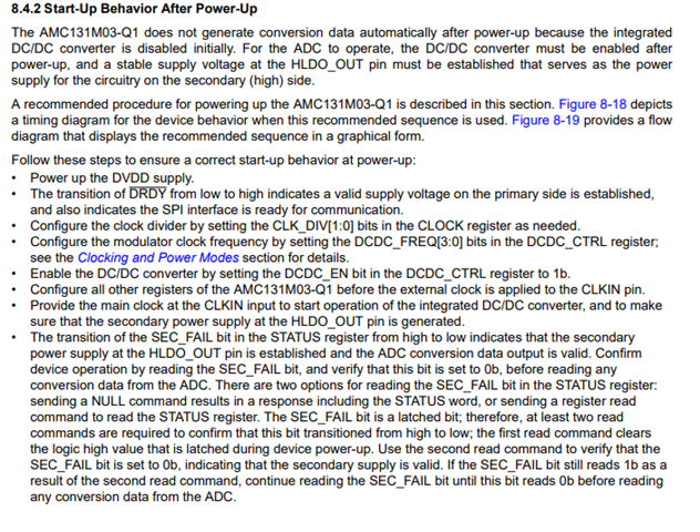
    On first time start-up you should do the following:

    In this case, once DVDD is stable the DRDY pin should go high.

    If you are resetting the device through a SPI write or the RESET pin, you will need the CLKIN signal to stay enabled.  The reset is timed with the CLKIN signal, so it needs to stay enabled to understand the command and control the DRDY signal. (note:  The DRDY signal may toggle several times while the reset is occurring.  You should verify the reset status with the Status register).

    Thanks.

  • Ok. Thanks, this makes sense.

    We don't care if the MCU is reset by poweron or by other sources. It is obvious that the reset pin needs CLKIN when it is defined in CLKIN pulses, I just didn't realize. I will try to check the status instead.

  • Hello Ahmad,
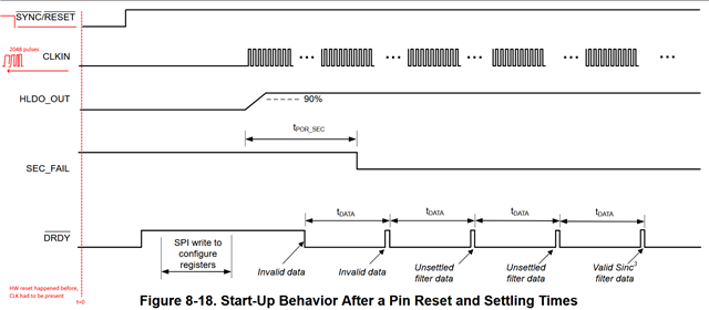
    In the DS chapter 8.4.3 figure 8-18 it is clearly visible, that even in case soft reset triggered by pin reset or reset command, the CLKIN signal should not be present. Could you please confirm then, that this is a mistake in datasheet and you are going to correct it?
    Best regards,

    Ivo

  • Hello Ivo, Hello Tomas,

    I would like to slightly correct the statement from my colleague.

    The AMC13xM0x devices have two sources of reset, hardware (HW) and software (SW) - over SPI. The HW reset requires toggling the SYNC/RESET pin. This reset uses the CLKIN clock domain for resetting the IC as my colleague pointed out. 

    Software reset

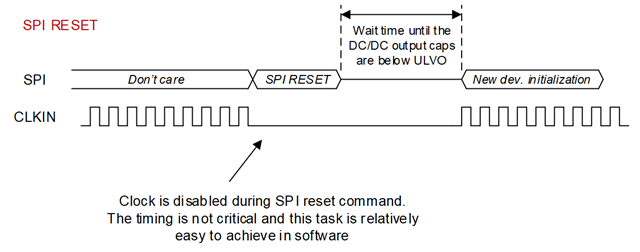
    SW reset happens over SPI command and DOES NOT use the CLKIN clock domain. The CLKIN shall be disabled before sending this command (to be explained later).

    Hardware reset

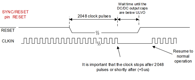
    The Figure 8-18 in AMC131M02 datasheet somehow indicates that the clock is not present during the reset. However, this figure shows rather "after reset" condition. See my hand-made modification.

    It is important, that during the HW reset, the clock stops after 2048 pulses, worst case, 2048pulses + 5us.

    Explanation:

    • The software reset, or reset through the SYNC/RESET pin, resets only the primary (MCU) side of the AMC131x device.
    • The reset of the MCU side brings registers to the default configuration.
    • The default configuration disables the integrated DC/DC converter.
    • The secondary side (analog inputs) can be reset only through the Power-on reset (POR) when the DC/DC stops working.
    • It is important that the voltage on the output of the DC/DC converter drops below POR threshold before the customer re-enables the DC/DC converter.
    • The exact timing is depends on the capacitance on the output of the DC/DC converter.
    • A bleeding resistor may be added to speed-up this discharge.

    If you keep clocking the device through the CLKIN pin during the HW reset action (2048 clocks + 5us), the secondary side (analog inputs) may enter a low-power mode with very low current consumption (tens of nA). In this case, it takes long time to bring the secondary side voltage below the POR reset.

    Recommendation:

    Irrelevant of the reset source, make sure that the voltage on the secondary side (HLDO_IN) drops below 1.7V (2V nominally) before you re-enable the DC/DC converter over SPI during the device configuration.

    If you insist on using the HW reset, and you can't control the number of CLKIN pulses precisely (quite difficult task for the MCU), add a 3.6k bleeding resistor on the HLDO_IN. In this case, even if the device enters the low-power mode on the secondary side, you can calculate how quickly the secondary side drops below POR threshold based on the bleeder resistor and capacitance on the output of the DC/DC.

    Let me know if you want to discuss this more in detail.

    S pozdravem / Best regards

    Jiri Panacek

    Systems Applications Engineer, Isolated Converters

  • Hello,

    Thank you very much for this detailed answer!
    We have already PCB in production, so it is too late now to add the bleeding resistor. So I expect in case we re-enable DC/DC too early, it will not work properly. Is there any risk of damage or too high voltage?
    We can also add longer delay and rely on the bleeding of capacitors, but this would delay startup, so I would prefer not to use it in case it is not critical. 

    From your explanation about the reset sequence my conclusion is that it is easier to use software reset using SPI command and not the SYNC/RESET pin. 

    Best regards,
    Ivo

  • Hello Ivo, 

    Your understanding is correct. The software reset sequence is safer as the timing remains always the same and the analog inputs side (secondary side) of the isolated device never enters this ultra low Iq mode (tens of nA of consumption).  

    "So I expect in case we re-enable DC/DC too early, it will not work properly. "

    - to correct the sentence "it may not work properly". In most cases it will...

    Long story short:

    - you should avoid the low-iq mode as in this mode the discharge of the DCDC_OUT capacitors takes way longer

    - I still recommend waiting long enough for the secondary side going through UVLO. If all channels are disabled and CLKIN is disabled, the secondary side will still consume more than 800uA of current. With this information you should be able to calculate the time you need to reach the UVLO on the secondary side. 

    S pozdravem / Best regards,

    Jiří Panáček