Other Parts Discussed in Thread: ADS1261
Tool/software:
Hello,
I am working with the ADS1261 to measure a 3-wire PT100 RTD using the universal RTD circuit with low-side reference described in the TI RTD Reference Design Guide. My setup uses:
-
Reference resistor: 350 Ω between REFP0 and REFN0
-
RTD connection: AIN2, AIN3, AIN5 as per TI’s 3-wire low-side reference schematic
-
Capacitors: 220 nF from each analog input to AVSS as shown in TI’s circuit diagram
-
IDAC configuration: IDAC1 and IDAC2 both set to 3 mA and routed to AINCOM
-
Reference setting: Internal reference enabled (REF register: RMUXP=10, RMUXN=10, REFENB=1)
-
Mode: PGA bypassed, SINC1 filter, 1200 SPS, pulse conversion mode, chopping enabled
The initialization sequence is:
-
Configure REF, PGA, MODE0..3, IMUX, IMAG, INPMUX registers
-
Route IDAC currents to AINCOM
-
First measurement: AIN2 – AIN3
-
Second measurement: AIN3 – AIN5
-
Final RTD value = (first reading – second reading)
The problem:
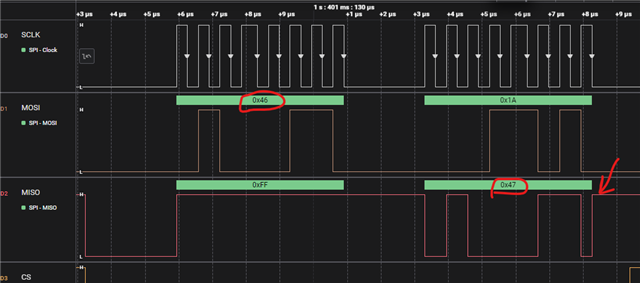
Even though the actual RTD resistance is ~330 Ω and I measure ~1.79 V across it with a multimeter, the ADS1261 conversion always returns 0 (status byte + all data bytes 0x00), except for the status byte which shows 0x04.
Questions:
-
Could the 220 nF input capacitors be causing the ADC to output zero if I don’t allow enough settling time?
-
With this topology, should I be using the internal reference (REF register) or routing to the external reference resistor voltage?
-
Is there any additional settling/conversion sequence required when switching the INPMUX channels in this universal RTD circuit?
-
Are there any known issues if START pin is held low and conversions are started via command mode only?
Any insights on what could be causing constant zero readings would be greatly appreciated.
Thank you,
Prashant V Achari