This thread has been locked.

If you have a related question, please click the "Ask a related question" button in the top right corner. The newly created question will be automatically linked to this question.

ADS1256: Serial communication Doubt

Part Number: ADS1256
Other Parts Discussed in Thread: ADS1255

Tool/software:

I am trying to develop and FPGA-based driver for the ADS1256 but in serial communication I have some doubts about the timing requeriments:

1.- t11 and t6 in commands RDATA, RDATAC and RREG are confusing. Please anyone can explain me the difference between them. 

2.- bit order (bit3) in the status register, says the following: Input data is always shifted in most significant byte and bit first. Output data is always shifted out most significant byte first. The ORDER bit only controls the bit order of the output data within the byte.

In terms of command shifts, the FPGA-based driver must send the most significant bit of the command? the bit order not affects in the command shifts?.  

3.- Considering that timing requirements are met. I have the following command shift order (Please feedback is very appreciated):

  •  pull down CS input. 
  • select AINP and AINN by MUX register.
  • Select PGA by  ADCON register.
  • Enable buffer if needed by STATUS register. 
  • Star a complete self calibration (offset and full scale). 
  • Apply command SYNC, WAKEUP.
  • Apply command RDATC.

Please ane feedback is appreciated. 

best regards.

  • I forgot this doubt : 

    commands summarized in Table 24 control the operation of the ADS1255/6. All of the commands are stand-alone except for the register reads and writes (RREG, WREG) which require a second command byte plus data. Additional command and data bytes may be shifted in without delay after the first command byte. The ORDER bit in the STATUS register sets the order of the bits within the output data. CS must stay low during the entire command sequence.

    This fragment causes me confusion. what command applies for this? (Additional command and data bytes may be shifted in without delay after the first command byte)
  • Hi Jose de Jesus Colin Robles,

    Answers to your questions:

    t11 and t6 in commands RDATA, RDATAC and RREG are confusing. Please anyone can explain me the difference between them. 

    Time t6 indicates the time between data being shifted into the ADC on DIN and the response data being shifted out of the ADC on DOUT

    Time t11 indicates timing restrictions between subsequent commands on DIN. So if you issue a WREG command for example, once you have completed the WREG command you must wait 4 tCLKIN before issuing the next command

    bit order (bit3) in the status register, says the following: Input data is always shifted in most significant byte and bit first. Output data is always shifted out most significant byte first. The ORDER bit only controls the bit order of the output data within the byte.

    In terms of command shifts, the FPGA-based driver must send the most significant bit of the command? the bit order not affects in the command shifts?.

    I would not worry about this bit and just leave it as the default. This way the first byte you receive from the ADC will be in this bit order 23-22-21-20-19-18-17-16 instead of 16-17-18-19-20-21-22-23

    Considering that timing requirements are met. I have the following command shift order (Please feedback is very appreciated):

    I would use SDATAC mode and the RDATA command instead of the RDATAC mode (not clear to me what you are doing since you wrote "RDATC")

    This fragment causes me confusion. what command applies for this? (Additional command and data bytes may be shifted in without delay after the first command byte)

    This just means there are no timing restrictions between the 1st command byte and subsequent command bytes, which only affects the WREG and RREG commands

    -Bryan

  • Hello Bryan thanks for your help, 

    I succesfully made the serial communication with the ADC. I would like to share for anyone the following recomentation: 

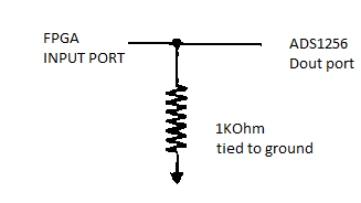
    FPGA connection with Dout port must be tied to ground using a 1KOhm resitance

    Maybe the FPGA port is not compatible with the ADS1256 Dout port. I share waveform of Dout in the Oscilloscope

    FPGA port connected to Dout, tied to ground: 

    Dout directly tied to FPGA port with no resistance.

    Any suggestion to avoid the use of the resistance is very appreciated.

  • Hi Jose de Jesus Colin Robles,

    You are showing that there is something pulling up / pulling down the DOUT pin when it is not being driven by the ADC. Whatever it is looks to be very weak as the rise/fall times look to be very long. But this is not an inherent characteristic of the ADC, it is something on that pin in the system

    Adding the 1k pull-down is overcoming whatever that weak driving source is to keep the DOUT pin low whenever the ADC is not driving it

    You might consider increasing the resistance value if possible, 1k is a little low for a pull-down. Maybe 10k?

    -Bryan

  • Hello Bryan I was using the comand RDATA triggered by an expernal push button, I do not why the Dout pin in the ADC show this behavior but with the pulldown resistance the voltage is driven to ground when the converter is waiting for another trigger singal. Here I put the siganl DRDY with the signal Dout with a data rate of 30KSP using the comand RDATAC. 


    using a 10Kohm resistance the last bit in Dout shows this

  • Hi Jose de Jesus Colin Robles,

    This looks better, I am glad we could help resolve the issue

    -Bryan