


Other Parts Discussed in Thread: ADC12QJ1600
Tool/software:
Hello, I have a few quick questions regarding my implementation of the TI-JESD204-IP, as someone inexperienced in this area of work.
1. First, I had a similar problem to that described here (e2e.ti.com/.../adc12qj1600evm-zcu102_8b10b-reference-design-not-showing-debug-cores), where debug cores were not visible after device programming. The reply to this made me assume that I would need an active external clock from a signal generator supplied to the ADC board (ADC12QJ1600), connected to my FPGA to make these cores visible, is this correct, or is it resolvable within the reference design provided?
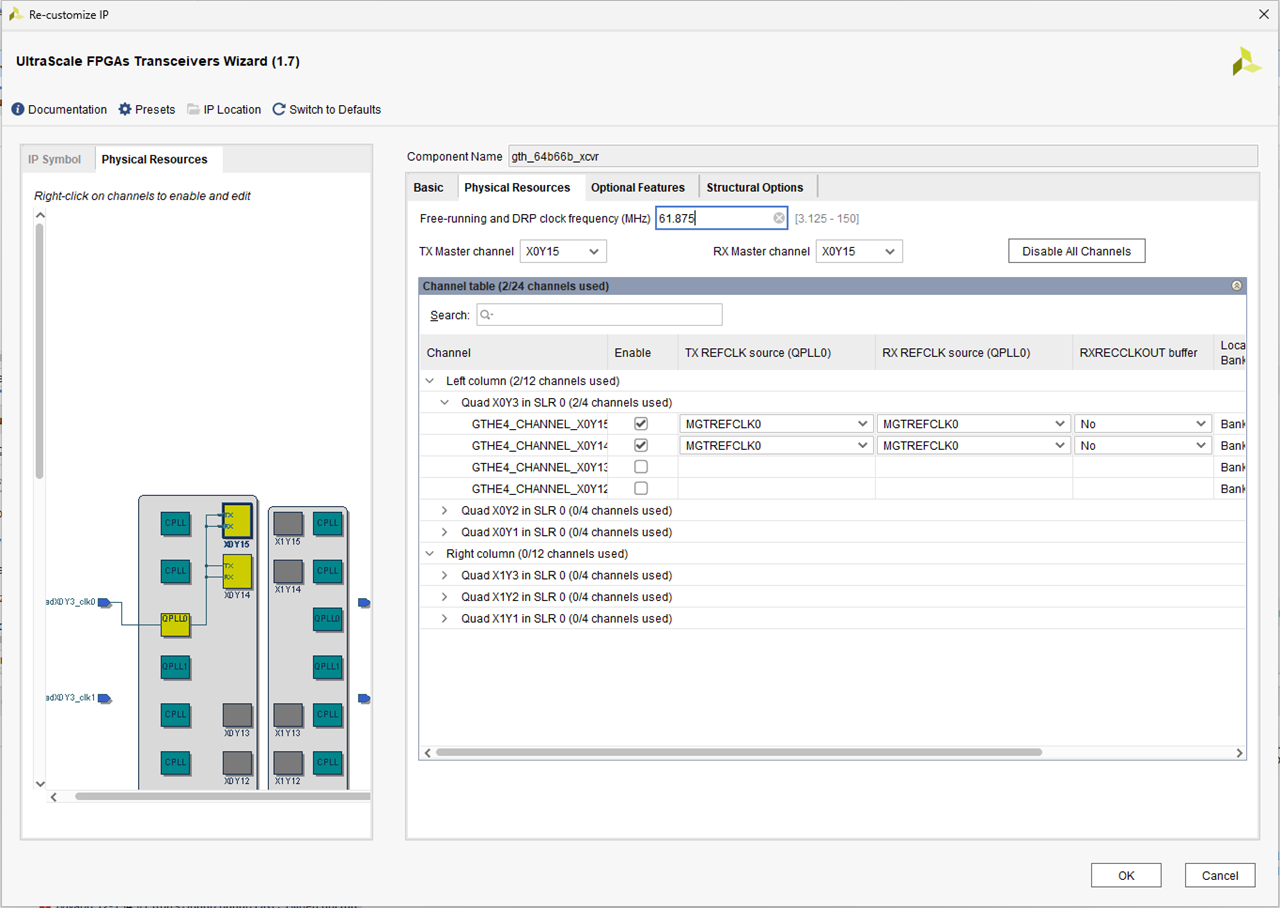
2. I also attempted to try a 2 lane receiver configuration. Am I correct in thinking it is as simple as configuring the transceiver wizard to two lanes as I have below, then setting NUMBER_OF_QUADS to 1 and NUMBER_OF_TX_LANES, NUMBER_OF_RX_LANES, lane mapping and lane polarity values accordingly in the relevant files?
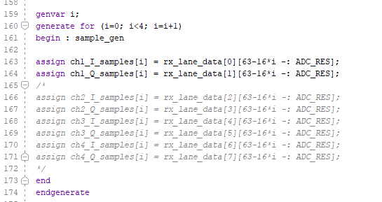
I also needed to omit the below section of code within the refdesign_rx.sv file to resolve errors. I just wanted to confirm if this was correct and that it will not contribute to any wrong results, as I did not find anything specific on this in the TI204c-IP users guide.
3. After implementing the reference design, even without any additional customization, there were many listed warnings (close to 1000) as below. Can I assume that these are negligible, as the impression I got was that there was no additional work needed for a working implementation that did not require customization?

Thank you.
