AFE58JD48: How to set the Total gain

Part Number: AFE58JD48

Tool/software:

Hi everyone,

I work currently on a project which integrate an AFE58JD48 in our board. I use an FPGA to do SPI communication with the AFE58JD48.

-> when I write register on VCA part (addr 0xC5 to 0x75E4), (addr 0xd1 to 0x588c), to set LNA=15DB,PGA=18DB,VCNTL=-0.31V, The corresponding total gain in the picture is 0DB, but my actual simulation is -6DB.

Under the settings of other LNAs, PGAs, and VCATs, the total gain is always 6dB less.

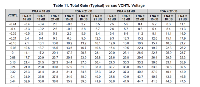
I couldn't find any more registers that need to be configured in the manual. How should I correctly configure the VCA registers? Could you provide me with a correct configuration?

Thanks for your help

  • How are you checking the actual gain ? How are you simulating this ?

  • I input a sine wave signal of 1Vpp using a signal source, and configured the amplifier to approximately 0dB according to the above settings. Theoretically, the signal range captured via Vivado should be 0-65535, but the actual range of the captured values is 16384-49152.

  • Hi,

    At 15dB gain you can give max of 0.71Vpp signal, If you give more than that signal chain will saturate . 

    To check the gain you can give smaller input and check the output . Are you using active termination or passive termination on board ? Please use the signal at device input while calculating the device gain.