ADC32RF55: SYSREF timing

Part Number: ADC32RF55
Other Parts Discussed in Thread: ADC12DJ2700, LMK04832

Tool/software:

Dear Person in Charge,

I am going to make a board using ADC32RF55 and evaluate its performance.
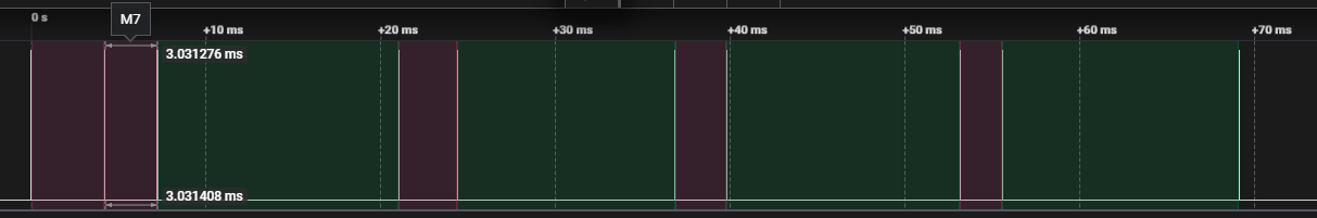
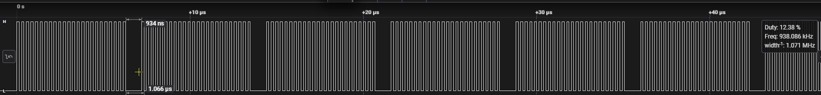
I have a question about the timing of SYSREF and device clock.

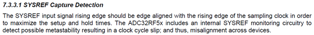
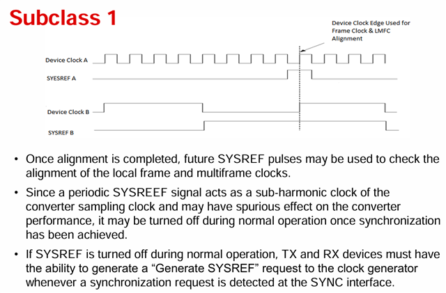
According to the section 7.3.3.1 of the ADC datasheet, it seems to mean that the rising edge of SYSREF should be aligned with the rising edge of device clock. Is this understanding correct?

On the other hand, looking at TI's other documentation, it appears that SYSREF is being triggered when the device clock falls.
Which is correct?

Thank you.

Best regards,

Sayaka Kose

  • Hi Sayaka,

    The sysref is on the rising edge for this device. The second figure you show indicates that the SYSREFB changes from low to high on the falling edge as this is the best time to ensure to stray sysref occurs from setup/hold timing. The SYSREFB is latched on the clock rising edge as shown.

    To synchronize the ADC32RF55, you must supply a common SYSREF as well as a source synchronous clock input to both devices. The device requires SYSREF during bringup sequence in a few places to synchronize internal blocks. If these blocks are not synchronized across the ADCs at the same time, then you may not achieve true synchronization.

    Thanks, Chase

  • Thank you for your reply, Mr Chase.
    In other words, the rising edge of SYSREF and the device clock must be aligned.

    I would like to ask an additional question.

    ① What is the correct value of register 0x22F on the ADC digital page?
    I know that the ADC contains a SYSREF monitoring circuit to monitor the positional relationship between SYSREF and the device clock.
    For example, if the SYSREF and the rising edge of the device clock are aligned correctly, what value is returned to 0x22F? how should I use this register?

    ② What is the CAL_STATUS of register 0x298 on the calibration page?
    The JESD communication between the ADC and the FPGA on the receiving side is not working well, and when the value of 0x298 is read, 0x1 is returned, so I assume that calibration is not completed.
    I know that 0xE is returned as a correct value, but is there any meaning to the value returned when calibration fails? In other words, what does 0x1 mean?
    And I am sorry to ask a basic question, but what exactly is the situation when "calibration is completed"?

    Thank you and best regards,

    Sayaka Kose

  • I would like to ask an additional question about ③.

    The ADC on the board I designed seems to have failed calibration.
    What could be the cause of the failure?
    In addition, although the device is different, the calibration was completed by increasing the delay output by the tool in the thread below.
    Is the above solution effective for ADC32RF55?

    ADC12DJ2700: FG calibration failure - Data converters forum - Data converters - TI E2E support forums

  • Sayaka, if you are using a single device then the system edge and monitoring does not matter unless you are required to have deterministic latency for the link bring up. You can leave sysref monitoring alone. It will report whatever your monitored sysref window is at that instance. It is not sticky bits meaning you read it twice back to back it may have different results. There is a whole section of the datasheet explaining the sysref windowing feature if you are interest in using it. It's meant for systems with a slow sysref edge relative to the sample clock and can be used to adjust the sysref relationship to the ADC clock internal to the ADC.

    Calibration only fails if there is not a sample clock present or the calibration status read back is read during the calibration, meaning you didn't wait long enough to read it back. This most likely is due to incorrect implementation of delays in your spi controller. Any value other than 0xE for the lower 4 bits of that register mean the calibration failed or is incomplete. Calibration being complete means the internal calibration loop of the ADC has converged and has settled. This is why there is a longer delay required at the end of the sequence because it takes a while for the calibration loop to settle.

    ADC12DJ2700 has nothing in common to the ADC32RF55. Using the delays from the GUI tool will have the ADC pass calibration every time.

    Thanks

  • Thank you for your reply,

    I understood about SYSREF, thank you. On the other hand, I don't do understand about calibration and would like to ask you.

    In our system, an FPGA is used to configure LMK04832 and ADC32RF55.
    After powering up LMK and ADC, the FPGA first writes the configuration sequence to LMK. After the sample clock (2.5 GHz) and SYSREF (about 1.22 MHz) are output from LMK and the FPGA confirms that the PLL inside LMK is stable, the design sequence is written to ADC. At this time, we use the register output by the GUI tool to write to ADC. However, the delay output by the tool is 0.1 s, so we change it to 1 s and use it. Is this correct? And when the sample clock is 2.5 GHz, the tool waits for about 1.5 s as the calibration wait time, so our system includes 1.6 s as the calibration wait time.
    I think the evaluation board also writes to ADC after writing to LMK. What is the approximate delay between writing? I would like to know the reasonable delay time between the sample clock input and writing the settings to ADC. (Of course, I know we need to take into account things like wire length delay, so approximate is fine.)
    Also, what is the SPI communication frequency to ADC register of EVM? Our system communicates at 1MHz. Is it possible that this value is too early or too late?

    Thanks and best regard,

    Sayaka Kose

  • Hi Sayaka,

    The tool takes 223ms on average between the last LMK register write and the first ADC register write. The GUI SCLK frequency is approximately 3.75MHz.

    However, the nature of calling a DLL for each register operation as our tool does the minimum delay between any sequential spi transaction seems around 3ms. Due to the added step of read and modify before the next register write can occur, the delay between any two register write operations is around 16ms (red + green regions) if the register has to be manipulated.

     The transaction below shows the following sequence:

    ADC32RF55.write(0x005,0x00)
    ADC32RF55.write(0x005,0x40)
    ADC32RF55.read(0x06D) = 0x00
    ADC32RF55.write(0x06D,0x40)
    ADC32RF55.read(0x06D) = 0x40
    ADC32RF55.write(0x06D,0xC0)
    ADC32RF55.read(0x06E) = 0x00
    ADC32RF55.write(0x06E,0x01)
    ADC32RF55.read(0x06E) = 0x01
    ADC32RF55.write(0x06E,0x03)

    So if just using the generated register sequence, then the GUI transactions for any two sequential writes will occur on average every 3ms.

    I have just added a feature such that the imported sequence is much faster now than before. Instead of being the same 3ms delay between two register writes, I have made it so now I perform the register operations in chunks without making multiple calls to the DLL. This made it such that sequential writes to the ADC occur with a delay of 1us now, yes 1us. This still works to program the ADC and performance looks as expected. I think any issues you are facing is due to clock related or again due to delay problems.