ADC32RF55: LMK04832 divider setting on ADC3xRF5xEVM--GUI

Part Number: ADC32RF55
Other Parts Discussed in Thread: TSW14J58EVM, ,

Tool/software:

The ADC is evaluated using ADC32RF55EVM and TSW14J58EVM.
ADC3xRF5xEVM-GUI tool is used to set the register to ADC.
I have the following questions.

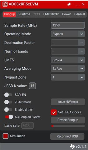
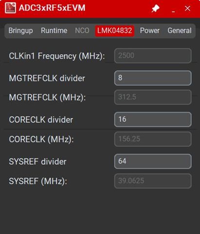
① I want to run FPGA with original implementation, but the value of divider in LMK setting is automatically 8/16/64 when BringUP. Do I have to change the receiver (FPGA) with this condition?

Why is it forced to this value during BringUP? Is the reason a constraint on the ADC32RF55 side? Or is it an EVM specific constraint?

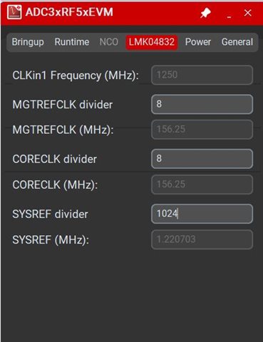
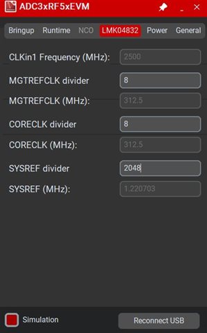
② I know that if I change the value of LMK page after BringUP, the value of SYSREF etc. will be changed. For example, if I want to proceed with the value of each divider at 8/8/2048, is there no problem with the following procedure? Is there any other necessary procedure?

[Procedure]
・Use ADC tool to DeviceBringUP
・Set LMK to 8/8/2048.


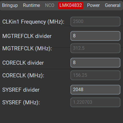
・Write FPGA to TSW・・・EVM evaluation board.
・Press Toggle SPI SYNCb.

③ When running ADC32RF55 using the original board, should the divider value of LMK setting be designed to be 8/16/64 during BringUP? Should we not design an arbitrary divider value from the beginning?

Thanks and best regards,

Sayaka Kose

  • The GUI is setup to work with TSW14J58EVM out of the box for easy eval. You can change LMK divider afterwards to work for your setup. Alternatively program LMK first and uncheck the Set FPGA Clocks option before Device Bringup. It will not program LMK with values meant for TSW14J58EVM and HSDC Pro evaluation. 

  • Thank you for your reply, Mr. Chase.

    You can set the value as you like. However, I have not been able to do it.
    Please let me share the information and reason why I failed.

    Situation (1) The sample clock is 1.25Gsps, the divider value is 8/8/1024, and K=16.

    Data acquisition succeeds.

    Situation (2) The sample clock is 2.5Gsps, the divider value is 8/8/2048, and K=16.

    Data acquisition fails.

    Situation (3) The sample clock is 2.5GSPS, the setting that matches Set FPGA Clocks (Divider value is 8/16/64, K=16).

    Data acquisition fails.

    *At the time of this writing, Set FPGA's clocks is turned off. The settings other than Sample Rate and Clock Division Ratio have not been changed, and the procedure is as instructed.

    Also, I look forward to your reply to the forum I posted.

    ADC32RF55: SYSREF timing - Data converters forum - Data converters - TI E2E support forums

    Thank you and best regards,

    Sayaka Kose.

  • Sayaka,

    This is only half of the information. The LMK register settings of the GUI definitely work as intended. Your fpga is expecting specific frequency as transceiver reference clock and as the core clock. If you do not provide the correct values then the capture will not occur. You must determine and set these divider values on your own. I just expose the ability for you to do it easily with the GUI tool if using our ADC EVM for evaluation.

    Thanks 

  • Thank you for your reply,

    I know that "my fpga is expecting specific frequency as transceiver reference clock and as the core clock ", so The FPGA is rebuilt every time to match the input clock setting.

    When I set the LMK's clock 2.5Gsps, the divider value is 8/8/2048, I also set the FPGA's setting to the same.

    The settings on the FPGA side and the LMK side are the same each time, but as you can see above, the data acquisition succeeds or fails depending on the settings.

    I hope your support.

    Thanks and best regard,

    Sayaka Kose