This thread has been locked.

If you have a related question, please click the "Ask a related question" button in the top right corner. The newly created question will be automatically linked to this question.

ADS1262: Input impedance variation

Part Number: ADS1262


Tool/software:

Hi,

We have been using the ADS1262 on a datalogging product successfully for a few years. A recent batch of boards, which have this part fitted, have all exhibited a wildly different input impedance from those we've had previously. This is adversely affecting some modes of operation of our product. The datasheet only indicates a typical differential impedance (when using the PGA, which we are) of 1GΩ, which is approximately what we have found in the past. This recent batch have an input impedance of around 30MΩ, (which, incidentally, is closer to the published spec when bypassing the PGA, which we're not doing). This is nearly two orders of magnitude different, which is not what I would anticipate as being a reasonable variation from a 'typical' specification.

All the devices have the following markings:

1262
39KG4
AHPV

Has there been a recent change that could explain what we're seeing?

Thank you,

Brian

  • Hi Brian Marriage,

    Can you tell us how are you measuring the ADC input impedance? 

    Also, can you confirm that the register reads and writes are working correctly in the system (I assume they are since this is a legacy system)? If so, can you read back the MODE2 register to confirm that the PGA is enabled and not bypassed? Please share a logic analyzer capture

    -Bryan

  • Hi Bryan,

    Thank you for your prompt assistance. I wish I had spent some more time investigating rather than jumping to conclusions. It turns out the input impedance is actually fine. That diagnosis had come from an observation that the error was only appearing during resistance measurements. We've now confirmed that it is as expected. In answer to your question, I did also verify that the PGA was enabled.

    We first discovered the problem in the situation where we measure resistance, where we use the PGA and also a separate 3v reference (which is not as stable as the internal one). At the top end of our 300kΩ range, we encountered a measurement error of around 3kΩ, where we'd normally expect this to be less than 40Ω. After verifying this as a reference offset error, we simplified the arrangement and removed both the PGA and the external reference from the experiment.

    Our investigations indicate that there is actually an offset (even with the internal reference) of approximately 2mV when the input MUX is routing it to the ADC. If we feed the reference output (REFOUT) straight back into the ADC inputs (we used REFOUT to AIN6, and AVSS to AIN7), we expect to get a full-scale reading. Note we have to disable the PGA in this test due to exceeding the voltage input range of the PGA.

    INPMUX 0x67
    IDACMUX 0xBB
    IDACMAG 0x0
    REFMUX 0x0

    Our board has 2x ADS1262 fitted. For our tests, one is an older, 'working' example (markings '1262' '9BKG4' 'A2P7') and the other is a recent 'problematic' example (markings '1262' '39KG4' 'AHPV'). They are wired identically.

    When reading the value back from each ADC, the 'working' device repeatedly gives the correct result: 0x7FFFFFFF

    The 'problematic' one gives lower values:
    0x7FE8560B
    0x7FE8570B
    0x7FE85925
    0x7FE856EA
    0x7FE8579D
    0x7FE85649
    0x7FE8542B
    0x7FE85696
    0x7FE856E4
    0x7FE85654
    0x7FE85864
    0x7FE85731
    0x7FE8566C
    0x7FE856A5
    0x7FE856BE

    ...which have an average of 0x17A92B below (or 99.93% of) full scale. At 722ppm, this is more than double the max spec of 300ppm of gain error (GE), and much, much more than we've ever seen before.

    It might be possible for us measure this error in our firmware and calibrate it out, but we don't know whether this error is stable over time or temperature.

    Any thoughts, questions, or suggestions of things to try much appreciated.

    Regards and thanks,
    Brian

  • Hi Brian Marriage,

    Are you performing an offset calibration first before taking these measurements? A positive offset and a positive gain error will give you a positive full scale code even when the input is slightly less than full scale. The opposite is true for a negative offset and negative gain error, which might be what is happening in your situation

    I'd also try using an external high accuracy reference source to achieve the same goal, and see if the numbers match. 

    -Bryan

  • Hi Bryan,

    Thanks for your suggestions.

    We do not use the built-in calibration system. The device has (until now) provided excellent and sufficient accuracy without it. Also, in some of our use-cases, we cannot afford the time (over one second for a complete calibration) during operation; and in other use cases we turn the ADC off regularly to save battery power and cannot afford the power drain from re-running the calibration when it is turned back on.

    I've run some tests today using a precision voltage source verified against a calibrated Fluke 8558A (with which I also accurately measured the ADC's reference). I also tried a zero input to confirm we're dealing with an gain rather than an offset problem (we are). Additionally, I tried a negative input and found the gain error was basically the same in that case.

    In both the positive and negative tests, I ensured that we weren't quite reaching full-scale. This verified that our older samples are behaving as we thought with the error within spec. But the newer ones are around ten times worse, which takes them well out of spec. Are you able to source samples of this batch and verify our findings?

    Thanks again,
    Brian

  • Hi Brian Marriage,

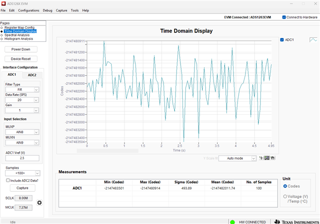
    I tried some tests on my EVM using the following settings / conditions:

    • AIN9 = REFOUT, AIN8 = ground
    • PGA = bypassed
    • Internal VREF
    • SINC4 filter, 100 SPS, measured 100 samples

    I then measured both AIN9-AIN8 (+2.5V) and AIN8-AIN9 (-2.5V). As you can see from the plots below, measuring 2.5V yields a positive full-scale signal just like you expect. However, measuring -2.5V yields randomly-varying codes that are near, but not quite at, negative full-scale. This indicates to me that this ADC has a positive offset and a negative gain error. I then measured an offset error of 57uV and a gain error of ~50ppm. As mentioned in my previous post, I assume you could have a similar situation.

    Can you try performing the same measurements on your board to see if the result is the same? You can then play around with the OFCAL and FSCAL registers to see if you can determine the actual offset and gain errors in the system. The offset can be measured directly by shorting the inputs to mid-supply. You can do this easily by setting MUXP=MUXN=REFOUT (you mentioned a "zero input", but it wasn't clear to me how you made this measurement and what the result was - there should have been at least some offset that needs to be accounted for). You can dial in the gain error using some math and a bit of trial and error once the offset is removed.

    I assume you are disabling the PGA for these measurements, because you must be applying REFOUT to AIN6 and then tying AIN7 to ground (or vice versa) - is that correct? The analog inputs cannot be connected to ground when the PGA is enabled

    MUXP = AIN9, MUXN = AIN8 (VIN = 2.5V)

    MUXP = AIN8, MUXN = AIN9 (VIN = -2.5V)

    We do not have a way to source units from a specific batch once those units get released by TI. There have been no recent changes to the ADS1262 production material

    -Bryan

  • Hi Bryan,

    Thank you for your efforts in trying to reproduce our problem, and apologies for being a bit light on the details in my previous message.

    I confirm that I disabled the PGA for all my tests once I'd determined it was unconnected with the problem we are seeing. I was using the internal reference, input chop enabled, the FIR filter, at 20 SPS. In all tests, the 'negative' input (AIN7) had a 10K pull-down to 0VA.

    For the zero tests, I shorted AIN6 and AIN7 together. The pull-down was still present. The error for good and bad ADCs were -133 counts and 121 counts respectively.

    In my 'positive' tests I was feeding +2.4500V into AIN6-AIN7. This was specifically to keep it below the internal reference (of +2.5V) so as not to lose errors that went above fullscale. I had around 25 samples in my dataset:

    Positive test 'Good' ADC 'Bad' ADC
    Ref (V) 2.49755 2.49592
    Min (codes) 2106738443 2106462181
    Max (codes) 2106747146 2106478889
    Average (codes) 2106742831 2106466908
    Expected (codes) 2106598441 2107974188
    Error (codes) -144390 1507280

    In my 'negative' tests I was feeding -1.6000V into AIN6-AIN7. Again, I had around 25 samples in my dataset:

    Negative test 'Good' ADC 'Bad' ADC
    Ref (V) 2.49755 2.49592
    Min (codes) -1375846671 -1375662105
    Max (codes) -1375840998 -1375656713
    Average (codes) -1375843780 -1375658629
    Expected (codes) -1375737757 -1376636204
    Error (codes) 106023 -977575

    As you can see, the error we're seeing from the 'Bad' sample is 10x worse. Is there any way I can send you some of our 'bad' samples so you can try them?

    Thanks and Regards,
    Brian

  • Hi Brian Marriage,

    Thanks for the feedback, can you please help with the following?

    1. Can you repeat these tests after removing the 10k resistor on AIN7 and instead just tying this pin directly to ground? Please also measure the ADC input voltage and reference voltage at the ADC pins using your 8.5digit DMM. I assume you have a cap across the reference and analog inputs, so you can just measure across this component. Please provide the raw ADC data in hex for all samples you take, instead of an average result
    2. Have you run these tests on any other "good"/"bad" ADC combinations? if so, can you share those results as well?
    3. You said you have two ADS1262 your board, and that you have been testing a single board with 1x "good" device and 1x "bad" device installed. Can you confirm that both ADCs have the exact same layout, BOM, etc.?
    4. Have you tried swapping the location of the ADCs on the board to see if the issue follows the device or the board?
    5. How many devices have you seen that have this issue? You mentioned "a recent batch", but can you quantify how many you've tested and confirmed have the issue?
    6. Do any of the new devices not show this issue?

    Once these questions are answered and actions completed we can decide how best to proceed

    -Bryan

  • Hi Bryan,

    Thanks for your questions. I have some responses...

    1. I've removed the 10K and grounded AIN7. There is 4.7nF across the input and 1uF across the reference.
    2. We have another board where we have fitted the 'good' and 'bad' the other way round. The (very similar) results below are from that board.
    3. Yes - the circuits are identical and the layouts are virtually identical.
    4. Yes - see 2.
    5. Every one of the batch that we have tried is misbehaving in this way. Our testing takes some effort and time, so we have paused that! I think we have at least 20 that we know to be bad.
    6. Not that we have found yet!

    Thanks again,
    Brian

    Results below...

    --------------

    BAD ADC
    REF: 2.496047v
    INPUT: 2.450000v

    7D8E23F0
    7D8E26F0
    7D8E157F
    7D8E0CD0
    7D8E2040
    7D8E1E43
    7D8E0D9B
    7D8E161A
    7D8E1E33
    7D8E1A6A
    7D8E0C8A
    7D8E1221
    7D8E2141
    7D8E18E9
    7D8E0AB5
    7D8E16A4
    7D8E2075
    7D8E1580
    7D8E1D42
    7D8E137A
    7D8E18D3
    7D8E19FD
    7D8E1C52
    7D8E1D2D
    7D8E2313
    7D8E13B4
    7D8E15B2
    7D8E1648
    7D8E1596
    7D8E1639
    7D8E0CA7
    7D8DFDC6
    7D8E14D2
    7D8DF753
    7D8E15B5
    7D8E1BD6
    7D8E05C8
    7D8E0E8D
    7D8E129D
    7D8E0769
    7D8E03C6
    7D8E0632
    7D8E0844
    7D8E0E02
    7D8E0DD0
    7D8E0AE4
    7D8E064E
    7D8E0B12
    7D8E183A
    7D8DFFC3
    7D8E0A2D

    --------------

    GOOD ADC
    REF: 2.498017v
    INPUT: 2.450000v

    7D8A02C3
    7D8A01B6
    7D89FE0F
    7D8A01FC
    7D89F82C
    7D8A12C1
    7D8A0D69
    7D8A1711
    7D8A018E
    7D8A1173
    7D89FD2D
    7D8A0A83
    7D8A0385
    7D8A1302
    7D89F787
    7D8A0B6F
    7D8A023F
    7D8A0A4E
    7D8A0AE0
    7D8A1199
    7D8A12FB
    7D8A08E9
    7D8A087E
    7D8A1094
    7D8A000B
    7D8A09CB
    7D8A0FB3
    7D8A0540
    7D8A0858
    7D8A1AB2
    7D8A1BEA
    7D8A14CD
    7D8A1B57
    7D8A0C28
    7D8A13CF
    7D8A0B22
    7D8A0DA7
    7D8A18D4
    7D8A0DDE
    7D8A0068
    7D8A0B6E
    7D8A0834
    7D8A0E7C
    7D8A0719
    7D8A1CB7
    7D8A1125
    7D8A147C
    7D8A171B
    7D8A1266
    7D8A142E
    7D8A07AB

    --------------

  • Hi Brian Marriage,

    Thanks for providing the requested information

    Let's start the process of sending some / all of these devices back to TI:

    -Bryan