Tool/software:
Hi!
We have observed two different voltage offset levels during bootup of ADS7142, that persists while the device is powered on, despite offset calibrations/software resets. These levels are 16 LSB apart, and the probability of the specific offset level occurring seems to depend on temperature. This offset seems to be very consistent and reproducible across different devices and even platforms, and translates to approximately 500uV after conversion. The offset is shared between the channels of a converter, but not between different converter units. Otherwise the offset calibration seems to be accurate up to 1 bit level.
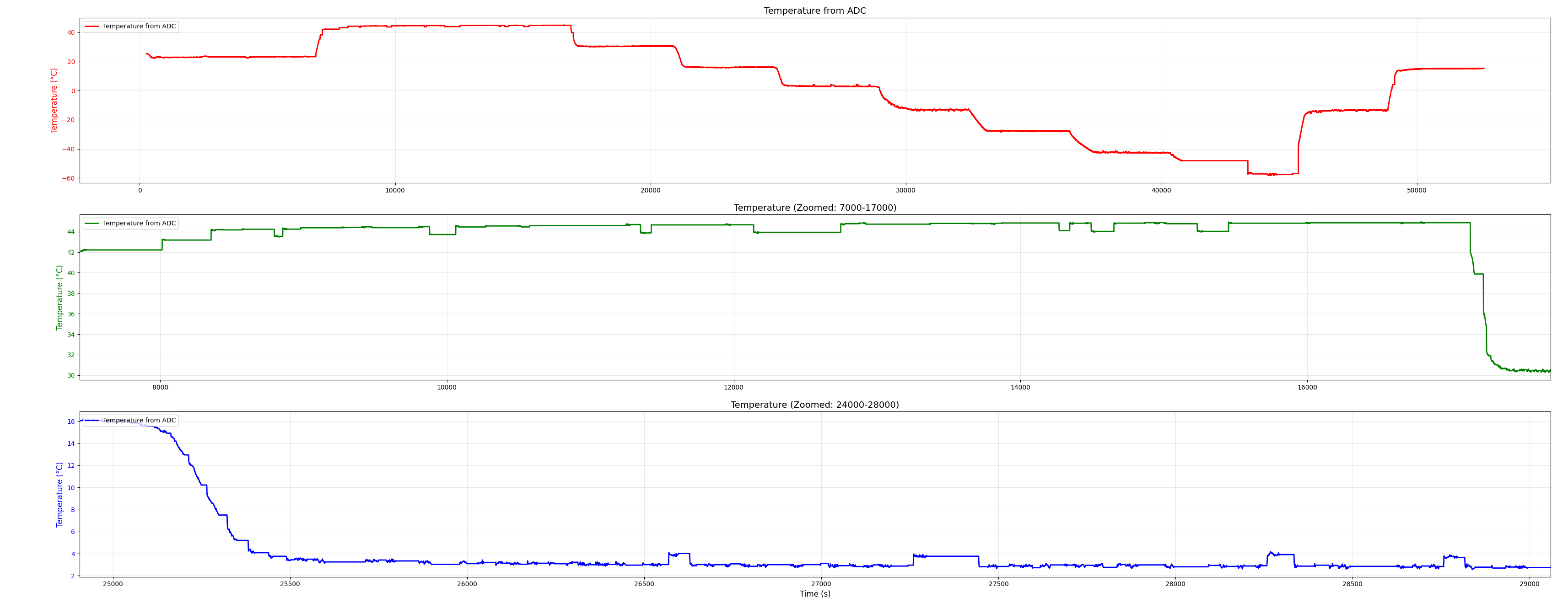
Below are some plots of the phenomenon. Note the difference in behavior when rebooting the device during test in Fig. 2. and when the device is powered for the full duration of the test in Fig. 3.
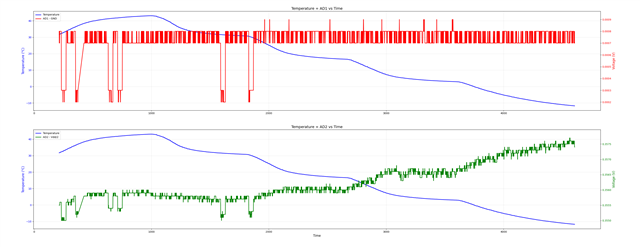
Fig. 1. Plot of a temperature sweep from 45degC to -10degC. The device is powered on and off periodically. AD1 is connected to GND and AD2 measures a node between two resistors. The resistors appear to have some temperature dependency.
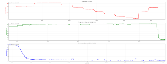
Fig. 2. Temperature measurements utilizing AD7142 AD converter. The device is powered on and off periodically. Voltage offset levels can be seen switching polarity based on temperature.

Fig. 3. Temperature measurements while the device is constantly powered on. The offset levels appear stable despite offset calibrations and software resets.
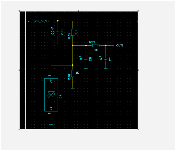
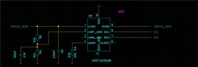
Here is our schematic around the AD converter. Note it is not possible for us to monitor the BUSY/RDY line.
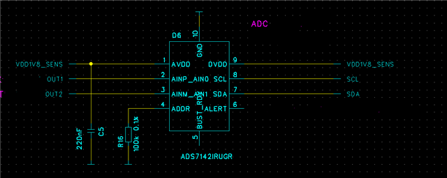
Fig. 4. Schematic around the converter.
We have tried the solutions provided in TI forums, but to no avail (software resets etc.) Furthermore, the phenomenon has been observed even when supplying ADS7142 power with a power supply. Different capacitor configurations around the converter has also been tried. This seems to have some effect on the distribution of to which offset the converter settles, but the phenomenon is observable nevertheless.
Below is our code for initialization:
void Init_ADS7142_PT1000_black_bright(){
	uint8_t ADS_COMMAND[4];
//	ADS7142_SoftwareReset(&hi2c1, ADS7142_I2C_ADDRESS_PT1000);
	/*Calibrate offset values*/
	ADS_COMMAND[0] = SINGLE_WRITE;
	ADS_COMMAND[1] = ADS7142_REG_OFFSET_CAL;
	ADS_COMMAND[2] = ADS7142_VAL_TRIG_OFFCAL;
	HAL_I2C_Master_Transmit(&hi2c1, ADS7142_I2C_ADDRESS_PT1000, ADS_COMMAND, 3, 10);
	HAL_Delay(10);
	/*Select channel input configuration*/
	ADS_COMMAND[0] = SINGLE_WRITE;
	ADS_COMMAND[1] = ADS7142_REG_CHANNEL_INPUT_CFG;
	ADS_COMMAND[2] = ADS7142_VAL_CHANNEL_INPUT_CFG_2_CHANNEL_SINGLE_ENDED;
	HAL_I2C_Master_Transmit(&hi2c1, ADS7142_I2C_ADDRESS_PT1000, ADS_COMMAND, 3, 10);
	/*Select mode*/
	ADS_COMMAND[0] = SINGLE_WRITE;
	ADS_COMMAND[1] = ADS7142_REG_OPMODE_SEL;
	ADS_COMMAND[2] = ADS7142_VAL_OPMODE_SEL_HIGH_PRECISION_MODE;
	HAL_I2C_Master_Transmit(&hi2c1, ADS7142_I2C_ADDRESS_PT1000, ADS_COMMAND, 3, 10);
	/*Select Auto sequence channel enable*/
	ADS_COMMAND[0] = SINGLE_WRITE;
	ADS_COMMAND[1] = ADS7142_REG_AUTO_SEQ_CHEN;
	ADS_COMMAND[2] = ADS7142_VAL_AUTO_SEQ_CHENAUTO_SEQ_CH0_CH1;
	HAL_I2C_Master_Transmit(&hi2c1, ADS7142_I2C_ADDRESS_PT1000, ADS_COMMAND, 3, 10);
	/*Select High speed oscillator*/
	ADS_COMMAND[0] = SINGLE_WRITE;
	ADS_COMMAND[1] = ADS7142_REG_OSC_SEL;
	ADS_COMMAND[2] = ADS7142_VAL_OSC_SEL_HSZ_HSO;
	HAL_I2C_Master_Transmit(&hi2c1, ADS7142_I2C_ADDRESS_PT1000, ADS_COMMAND, 3, 10);
	/*Select nCLK parameter*/
	ADS_COMMAND[0] = SINGLE_WRITE;
	ADS_COMMAND[1] = ADS7142_REG_nCLK_SEL;
	ADS_COMMAND[2] = 0x60; 				//default value 0x15 = 21 cycles
	HAL_I2C_Master_Transmit(&hi2c1, ADS7142_I2C_ADDRESS_PT1000, ADS_COMMAND, 3, 10);
	/*Enable accumulator*/
	ADS_COMMAND[0] = SINGLE_WRITE;
	ADS_COMMAND[1] = ADS7142_REG_ACC_EN;
	ADS_COMMAND[2] = ADS7142_VAL_ACC_EN;
	HAL_I2C_Master_Transmit(&hi2c1, ADS7142_I2C_ADDRESS_PT1000, ADS_COMMAND, 3, 10);
}
and reading:
for(int i=0;i<loopcount;i++){
		ADS_COMMAND[0] = SET_BIT_ADS7142;
		ADS_COMMAND[1] = ADS7142_REG_START_SEQUENCE;
		ADS_COMMAND[2] = ADS7142_VAL_START_SEQUENCE;
		HAL_I2C_Master_Transmit(&hi2c1, ADS7142_I2C_ADDRESS_PT1000, ADS_COMMAND, 3, 10);
		for (int k=0;k<3;k++){
			ADS_COMMAND[0] = SINGLE_READ;
			ADS_COMMAND[1] = ADS7142_REG_ACCUMULATOR_STATUS;
			HAL_I2C_Master_Transmit(&hi2c1, ADS7142_I2C_ADDRESS_PT1000, ADS_COMMAND, 2, 10);
			HAL_I2C_Master_Receive(&hi2c1, ADS7142_I2C_ADDRESS_PT1000, TEST, 1, 10);
//			printf("number: %d\r\n", TEST[0]);
			if (TEST[0] < 16){
				delay_us(20);
			}
			else{
				k=3;
			}
		}
//		HAL_Delay(1);
//		delay_us(20);
		/*Read ACC_0 MSB and LSB*/
		ADS_COMMAND[0] = BLOCK_READ;
		ADS_COMMAND[1] = ADS7142_REG_ACC_CH0_LSB;
		HAL_I2C_Master_Transmit(&hi2c1, ADS7142_I2C_ADDRESS_PT1000, ADS_COMMAND, 2, 10);
		HAL_I2C_Master_Receive(&hi2c1, ADS7142_I2C_ADDRESS_PT1000, TEST, 4, 10);
br,
Pauli