ADS127L11: ADC IC: Inquiry

Part Number: ADS127L11
Other Parts Discussed in Thread: ADS127L21, ADS127L18, ADS127L14, THS4561, THS4551, THP210, PGA855, INA851

Tool/software:

Dear Team,

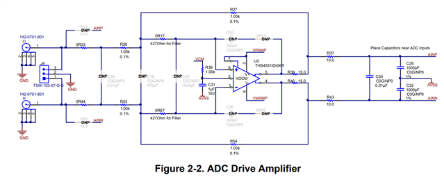
In my board I'm planning use the ADC ICs ADS127L11 for my application.

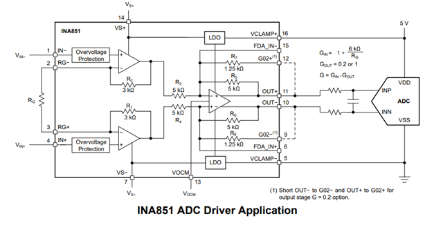
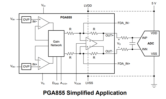
Can you suggest the output amplifiers that can be used for these ADC ICs.

Also there any other recommendations for my application.

My requirements are 1,2,4 or 8 channel ADC with sample rate 256KSPS, 24bit resolution ADC for medical applications.

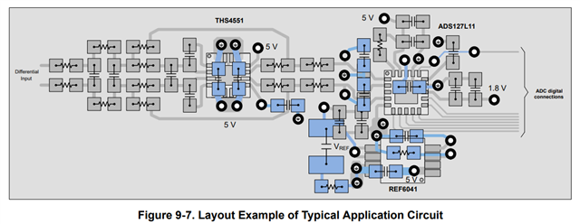
The size must be compact and less than 10mm*10mm.

Is there any specific recommendations for eliminating noise for signal integrity.

Regards,

Abhishek

  • Hello Abhishek,

    The recommendations for the ADS127L11 and ADS127L21 will be similar as the multi-channel ADS127L14 and ADS127L18 devices.

    If you need isolation between channels, then the single channel ADCs will be a better fit.  For multi-channel applications that do not require isolation, the multi-channel ADCs will result in a smaller board area per channel.

    There are several amplifiers suitable to drive the ADC inputs.  THS4551 and THS4561 are excellent choices, especially for input signal frequency greater than 20kHz.  If low frequency noise and DC accuracy are important, then the THP210 is another great choice.  These amplifiers are all fully differential, can operate from a single 5V supply, with an input impedance around 1kOhm typical for the THS4551 and THS4561, and 10kOhm for the THP210.

    The ADS127L11 evaluation board uses the THS4551, and can be used as a reference design.  Please refer to the ADS127L11EVM User's guide for more details.

    https://www.ti.com/lit/ug/sbau351/sbau351.pdf

    If you need high input impedance, then the INA851 or PGA855 can also be considered.  These amplifiers are high input impedance instrumentation amplifiers, but require a higher voltage supply than 5V.  If your system will be using +/-5V up to +/-15V supply rails for the input signal chain, then either of these amplifiers would be good options.

    For low noise designs, we recommend a solid ground plane, where digital and analog signals are kept separated in different areas of the board.  You can look at the EVM layout as a good guideline on how to layout and route a board to achieve low noise.  In addition, for low noise, it is critical that the power supply bypass capacitors are placed as close as possible to the ADC package.  The EVM and the applications section of the datasheet provide good layout recommendations.

    Regards,
    Keith Nicholas
    Precision ADC Applications