This thread has been locked.

If you have a related question, please click the "Ask a related question" button in the top right corner. The newly created question will be automatically linked to this question.

ADS1231: ADS1231

Part Number: ADS1231

Tool/software:

Dear Sir/Madam, 

We have used the device ADS1231 in our new design "PLC - Load Cell Input module".  This module provides one input channel to interface with a 4-wire or 6-wire strain gauge load cell sensor, supporting sensitivity levels from 0 to 3 mV/V.  

Currently, our design is in the final testing phase of R&D prototyping. During this phase, we have observed an issue: at room temperature (25C) the module output takes 30 to 60 minutes to stabilize, and the measured output count drifts from its initial value over this period. 

For example, we used a load cell calibrator to apply a 3 mV/V input to the module. For 3mV input applied, the expected digital output count for this input is 32,000. However, we observed that the count initially starts at approximately 32,001 and slowly increases, stabilizing at around 32,011 after 30 minutes. Please refer to the table below for detailed observations. 

Time (Minutes) Time (hh:mm) Analog input: 3 mV/V
Min Count Max Count
0 10.30 32001 32005
5 10.35 32003 32008
10 10.40 32004 32009
15 10.45 32005 32010
20 10.50 32006 32010
25 10.55 32007 32011
30 11.00 32006 32011
35 11.05 32007 32010
40 11.10 32007 32010
45 11.15 32007 32011
50 11.20 32007 32010
55 11.25 32007 32011
60 11.30 32007 32010

We would appreciate your guidance on the possible cause of this behavior. Specifically:

  • What might be causing the output to take 30 minutes or more to stabilize?

  • What could be contributing to the gradual increase in count values despite a constant input?

For your reference, we have attached the schematic diagrams for the ADS1231 circuit and the input channel.

We kindly request your feedback and support in resolving this issue.
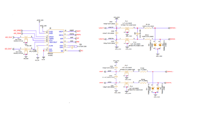
Best Regards

Rohidas Sawant 

R&D Dept.

  • Hi Rohidas Sawant76,

    Today is a national holiday in the US, please expect an initial response to your post in the next 1-2 days. Thanks for your patience.

    -Bryan

  • Hello Rohidas,

    This long settling time is likely due to dielectric absorption (DA) in the filter capacitors. Any ceramic capacitor greater than about 100nF will be a multi-layer construction and tends to have very high DA.

    https://en.wikipedia.org/wiki/Dielectric_absorption

    The filter capacitors in the input signal path as well as the CAP1 and CAP2 pins of the ADS1231 are all sensitive to DA.  All of these capacitors should be NP0/C0G type ceramic to minimize settling time due to DA.  It is likely the 1uF feedthrough capacitors are X7R type.

    1.  Verify the CAP1/2 capacitor and C60 differential AINx capacitor is NP0/C0G type.

    2.  The input signal is on the order of 100's to 1000's of ohms depending on the bridge resistance value and is more sensitive to DA.  In this path, remove the common mode 1uF feedthrough capacitors and check if this improves settling time.

    Regards,
    Keith Nicholas
    Precision ADC Applications

  • Dear Keith Nicholas

    Good afternoon!


    Thank you for your response.

    As mentioned in your email and shown in the images, we have removed the 1µF common mode feedthrough capacitors. However, we have not observed any improvement in the settling time performance.

     As per your suggestion, we will proceed with the other tests and share our feedback accordingly.

     In the meantime, we would appreciate it if you could suggest any other possible causes for the issue.

     Thanks & Regards

    Rohidas Sawant

  • Hello Rohidas,

    I should have looked more closely at the total code change.  I assume the codes you provided are direct codes from the ADS1231.  With a nominal code of approximately 32008, this translates to an input voltage of 74.524uV.  The average code change from time=0 to time=60min is approximately 6 codes, which translates to a voltage change of 14nV.

    The typical offset drift over temperature is 20nV/C, and can be higher for an individual ADC.  You could easily see a change of 0.5C or more over an hour in a typical lab environment or office setting.

    Also, any stress (pressure) applied to the board could cause small offset voltages in the capacitors or the ADC package, requiring many minutes or 10's of minutes to return to the initial state.

    Regards,
    Keith

  • Dear Keith Nicholas

    Good afternoon!

    Thank you for your response. I apologize for not providing sufficient details in my previous email. I had shared only a brief overview of the issue and observations. Please find below the detailed information regarding the setup, test procedure, results, and the issue we are encountering:

     Module Overview:

    Our Load Cell Interface Input Module supports one channel to interface with a 4-wire or 6-wire strain gauge load cell sensor, with a sensitivity range of 0.0 to 3.0 mV/V. The module provides a 5V DC excitation voltage, so the maximum input to the module is 15 mV.

    For a 15 mV input signal, the module's digital raw count is observed to be 6,623,529. Therefore, the raw digital count range for 0 to 15 mV input is 0 to 6,623,529. We scale this internally to provide a user output count from 0 to 32,000. Hence, at the maximum input of 15 mV, the expected user digital count is 32,000.

    Test Setup and Procedure:

    For testing, we used a load cell calibrator (UNIPULSE – 513B) as the signal source instead of a load cell sensor. The calibrator is set to 3 mV/V, which corresponds to a 15 mV input to the module. Therefore, the expected user output count should be 32,000.

     Test procedure and test result observations are as below:

    1. Calibrate the module using the UNIPULSE – 513B calibrator for the full range (0 V and 15 mV).
    2. After successful calibration, apply a 15mV input using the calibrator and observe the output count.
    3. Initially, the digital output is around 32,003 (fluctuating between 32,001 to 32,005).
    4. Maintain the 15mV input continuously for 60 minutes and observe the count at 5-minute intervals.
    5. We observed a gradual increase in the count. Around the 30-minutes, it stabilized at approximately 32,009 (range: 32,007 to 32,011), which is outside our acceptable range of 31,995 to 32,005.
    6. The issue is that the count stabilizes only after 30 minutes and increases by approximately 10 counts, which exceeds our tolerance.

    Modifications and Observations:

    We made several changes to the modules to investigate this issue further: 

    1. Modification:

    Change: Signal+ and Signal– input resistors (R105, R106) changed from 0Ω to 100Ω to match the 100Ω resistors on SENSE+ and SENSE–.
    Observation:

    • Recalibrated and measured.
    • Initial count: ~32,000 (range: 31,998 to 32,001).
    • After 30 minutes: ~32,002 (range: 31,998 to 32,004) — within acceptable range.
    • Note: This change was applied to two more modules, but no performance improvement was observed.


    2. Modification:

    Change: SENSE+ and SENSE– input resistors (R100, R101) changed from 100Ω to 0Ω to match the 0Ω resistors on Signal+ and Signal–.
    Observation:

    • Recalibrated and measured.
    • Initial count: ~32,000 (range: 31,997 to 32,003).
    • After 30 minutes: ~32,002 (range: 31,996 to 32,005) — within acceptable range.
    • Note: This change was also applied to two additional modules, but again no performance improvement was observed.


    3. Modification:

    Change: Same as Modification 2, plus capacitor C56 (across SENSE+ and SENSE-) changed from 47µF to 100µF.
    Observation:

    • Recalibrated and measured.
    • Initial count: ~32,000 (range: 31,998 to 32,003).
    • After 30 minutes: ~32,000 (range: 32,000 to 32,003) — within acceptable range.
    • Note: Applied to two more modules, but no consistent improvement was observed.


    4. Modification:

    As mentioned in previous communication, we removed SIGNAL+ and SIGNAL- feedthrough capacitors (FL7 and FL8), but no performance improvement observed.

    5. Modification:

    As per your suggestion, we will update the test result performance for CAP1/2 capacitor and C60 differential AINx capacitors NP0/C0G type.


    We would appreciate your guidance on the possible cause of this behavior. Specifically:

    • What might be causing the output to take 30 minutes or more to stabilize?
    • What could be contributing to the gradual increase in count values despite a constant input?
    • Why do the same modifications (1, 2 & 3) not consistently improve performance across different modules?

     We kindly request your feedback and support in resolving this issue.

     Thanks & Regards

    Rohidas Sawant

  • Hello Rohidas,

    Thank you for the additional information; this is helpful to better understand your test setup.

    The drift that you observe is much higher than expected.  Looking at the schematics again that you initially provided, it appears that you are using TVS diodes on the inputs for protection.  Normally, these devices can be used, but if I read your schematic correctly, you are using the 5V version.

    P4SMAJ5.0ADF-13 : Please confirm this is the correct part number.

    https://www.diodes.com/assets/Datasheets/P4SMAJ50ADF_P4SMAJ85ADF.pdf

    Taking a look at the datasheet, the maximum reverse leakage current of this TVS diode is 400uA.  In your case, you are operating at 2.5V, and the typical leakage current for these diodes will be much lower, but leakage current is probably in the 10's of uA.  Using a 350Ohm bridge, every 5nA difference in leakage current will result in 1uV of error.

    Please remove the TVS diodes from the Signal+/- inputs to see if this shows an improvement.  Even if this is not the source of error, I suggest you change these values to the P4SMAJ10ADF version, which has a maximum leakage of 1uA.

    Although not nearly as sensitive, the TVS diodes on the Sense+/- lines could also cause some change in readings, so I would recommend changing these to the P4SMAJ10ADF version as well.

    Regards,
    Keith

  • Dear Keith Nicholas San,

    Thank you for your valuable suggestions.

    We have removed the P4SMAJ5.0ADF-13 diodes from both the Signal+/- and Sense+/- lines. With this change, we observed some improvement in the readings at 25°C room temperature, and a significant improvement in readings during the 60°C high-temperature test.

     In addition to removing the diodes, we implemented the following two changes:

    1. Replaced 0Ω resistors (R105, R106) on the Signal+/- lines with 100Ω resistors.
    2. Replaced the 47µF/16V capacitor (C56) across the Sense+/- lines with a 100µF/10V capacitor.

    With these additional changes, we observed further improvement in readings at both 25°C and 60°C

    We would appreciate your feedback and guidance on the following points regarding these changes:

    Change 1: TVS Diode Selection:  Original: P4SMAJ5.0ADF-13 (5V)   Proposal: P4SMAJ10A (10V)

    Query:
    If we replace the P4SMAJ5.0ADF-13 (5V) diodes with P4SMAJ10A (10V) diodes on both Signal+/- and Sense+/- lines, will the ADS1231 IC inputs pins be protected during an ESD event or in the case of input voltages reaching the diode clamping level (~10V), which is above the IC’s AVDD supply (5V)?

    According to the ADS1231 datasheet, the maximum input current for the signal and sense pins is 10 mA.
    Will the combination of 100Ω series resistors and P4SMAJ10A diodes provide sufficient protection for the ADS1231 input pins, in compliance with IEC 61000-4-2 ESD standards?


    Change 2: Replacement of 0Ω with 100Ω Resistors (R105, R106) on Signal+/- Lines

    Query:

    • Is this change acceptable from a signal integrity and protection perspective?
    • If yes, what additional validation tests would you recommend to confirm and verify the impact of this design change?


    Change 3: Replacement of 47µF/16V Capacitor (C56) with 100µF/10V Capacitor on Sense+/- Lines

    Query:

    • Is this change appropriate in terms of noise filtering, stability, and performance?
    • If acceptable, what additional validation tests would you recommend to confirm and verify the impact of this design change?


    We look forward to your feedback and guidance on the above points.


    Best regards,
    Rohidas Sawant

  • Hello Rohidas,

    I am glad this improved measurement stablity.

    Change 1 and Change 2 Query:

    The 10V diode will clamp at a higher voltage depending on the magnitude of the ESD event; worst case you can use the Max clamping voltage of 17V.

    For ESD, the time width of the pulse will be on the order of 10's of nanoseconds, in which case we can use the 100mA peak rating of the ADS1231 input current.  For a safety margin, we should limit worst case momentary current to no more than 50mA.

    Rin = (Vpeak - Vmax)/Ipeak = (17V - 5.3V)/0.05A = 234Ohm.  Round up to 249Ohm input protection resistor for R105/R106.

    In reality, the filter capacitors will limit the maximum voltage to much less, acting as not only a noise filter but also a filter for ESD.  You will likely be fine if you keep the 100Ohm resistors, but further analysis may be required.  I suggest increasing to 249Ohm for more safety margin.

    Change 3 Query:

    The larger value capacitor will provide additional noise filtering and should not cause any stability concerns as long as the leakage current over temperature is small.  I would fully test the circuit over temperature to validate, but do not expect any problems with these changes.

    Regards,
    Keith

  • Dear Keith Nicholas San,

    Thank you for your valuable suggestions.

     We have implemented the following modifications:

    1. Replaced the diodes on the Signal+/- and Sense+/- lines (D12, D13, D14, D15) from “P4SMAJ5.0ADF-13” to “P4SMAJ10ADF-13”.
    2. Replaced the input resistors on Signal+ and Signal– lines (R105, R106) from “RES, SMD, MFR, 0Ω, 1%, 0805” to “RES, SMD, MFR, 100Ω, 0.5%, 1/8W, 25PPM, 0805”.
    3. Replaced capacitor C58 (connected to CAP1 and CAP2 pins of the ADS1231) from an X7R type “0.1µF, 50V, 10%, X7R, 1206” to an NPO type “0.1µF, 50V, 2%, NPO, 1206”

      Following these modifications, we conducted the following tests:

    1. Analog Accuracy Test: We tested the analog input accuracy at ambient temperatures of 25°C and 60°C. In both cases, the accuracy results were within the specified limits..
    2. ESD Testing: We performed ESD tests (contact discharge ±4kV and air discharge ±8kV) on the Signal+/- and Sense+/- lines in our simulation lab. The modules passed both contact and air discharge tests successfully.  

    Based on these results, the modified modules appear to meet both analog accuracy and ESD protection requirements.

    Please let us know if you have any comments on the above modifications and test results. Also, kindly advise if any additional validation tests are recommended to further confirm the impact of these design changes.

    Thanks & Regards

    Rohidas Sawant

  • Hello Rohidas,

    This is excellent news.  I do not have any additional recommendations at this time.  I can do a quick review of your board layout if you send an image that shows the ADC and all surrounding components.  The fact that you are able to pass ESD suggests that your board layout is already good.

    Regards,
    Keith